| Feb 01, 2012 |
Nanofabrication technique pushes recording density to 3.3 terabits per square inch
|
|
(Nanowerk News) The hard disk industry's success to continuously drive recording densities to new heights is owed to the use of granular media — nanoscopic magnetic grains that are weakly coupled and randomly arranged on the disk platters. Each individual bit of information is stored over an area containing tens of grains.
|
|
There are two common approaches to increasing the recording density of granular media: one is to reduce the grain size and the other is to reduce the number of grains per bit. Unfortunately, the general consensus is that both approaches will have difficulty pushing beyond the one terabit per square inch limit.
|
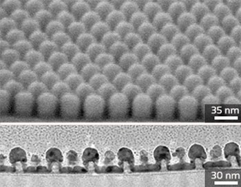 |
| Tilted-view scanning electron microscope (top) and cross-sectional transmission electron microscope (bottom) images of high-density bit-patterned media consisting of magnetic cobalt–palladium bits formed on hydrogen silsequioxane nanoposts defined by electron beam lithography. (© 2011 IOP)
|
|
Joel Yang at the A*STAR Institute of Materials Research and Engineering and co-workers from the A*STAR Data Storage Institute and other institutions have now come up with an alternative approach using so-called bit-patterned media (BPM) (see paper in Nanotechnology: "Fabrication and characterization of bit-patterned media beyond 1.5 Tbit/in2").
|
|
In contrast to granular media, BPM consists of ordered arrays of individual 'superbits' (see image) that are larger than the grains in granular media and can be individually addressed on a disk platter to improve signal-to-noise ratio. However, the fabrication of BPM requires lithographic patterning, a costly process that necessitates substantive viability studies to meet commercial requirements. Yang and his team have now demonstrated the fabrication of BPM with densities as high as 3.3 terabits per square inch — or 15 nanometer pitch — using a method that does not require pattern transfer processes such as etching and liftoff, which typically reduce pattern fidelity.
|
|
The new fabrication process involves only two steps. The first step involves the use of electron-beam lithography on hydrogen silsesquioxane resist to define silicon oxide nanoposts. "The resolution of our technique is higher than most electron beam lithography processes because we use a salt solution and development process that result in closely-spaced nanopost-resist structures down to a 15 nanometer density," says Yang.
|
|
The second step involves the deposition of cobalt–palladium films on top of the nanoposts to forming isolated magnetic bits (see image). "Because the nanopost resist is made of robust silicon oxide material, we can avoid the etching step by depositing magnetic material directly onto these nanostructures to form the magnetic bits," explains Yang.
|
|
The researchers used magnetic force microscopy (MFM) to analyze their BPM and found that the magnetic bits are magnetically isolated, thus able to store single bits of information, down to the best MFM-resolution of 20 nanometers. Yang and his team believe that the magnetic bits would remain isolated and individually controllable up to 3.3 terabits per square inch.
|