| Mar 12, 2012 |
Elucidation of the primary factor causing variability of characteristics in 14-nm-generation three-dimensional transistors
|
|
(Nanowerk News) Takashi Matsukawa and Meishoku Masahara, Silicone Nano-Device Group, at the Nanoelectronics Research Institute of the National Institute of Advanced Industrial Science and Technology (AIST), have elucidated the primary factor causing on-state current variability in 14-nm-generation three-dimensional transistors, i.e. FinFETs (fin field-effect transistors).
|
|
The factors that cause variability of on-state current in transistors are variabilities of threshold voltage, parasitic resistance, and trans-conductance. By analyzing the contribution of each of these factors in detail, the researchers have discovered that the primary factor causing variability of on-state current in the 14-nm-generation FinFETs is variability of trans-conductance. In addition, it was predicted that highly precise processing of silicon three-dimensional channels (fin channels) would reduce on-state current variability. Furthermore, a method of processing fin channels that is effective in reducing variability was proposed. The biggest problem in regard to the integrated circuits beyond the 14-nm generation, such as SRAM (static random access memory), has been reduced yield of the circuits. Since on-state current of transistors varying from the design level causes malfunction of the circuit, larger variability of on-state current reduces the yield. However, it is anticipated that the results of present research will help to solve this challenge.
|
|
The details of this technology were presented at the 2011 International Electron Devices Meeting (IEDM) in Washington, DC, USA on December 5-7, 2011.
|
|
Social Background of Research
|
|
The performance improvement and the integration scale increase of silicon integrated circuits have been achieved by miniaturizing the transistors, which are the smallest elements of these circuits. The miniaturizing of elements is also linked to cost reduction, and thus fierce competition to develop even more miniaturized elements continues. However, in the technology used for the 14-nm-generation transistor, which is expected to be in production after 2017, there will be issues with variability of characteristics among elements because of their small size, and there is concern about substantial reductions in product yields and reliability. In particular, SRAMs, which occupy more than 50 % of the area of system LSIs (large-scale integrated circuits) and microprocessors, can be easily affected by dispersion of characteristics owing to the intensive use of the smallest transistors in their circuits. For these reasons, there is a strong need to develop miniaturized transistors with small variability of characteristics.
|
|
History of Research
|
|
AIST has been conducting research in transistors with new structure called FinFETs that have a three-dimensional structure. In addition, AIST proposed a four-terminal FinFET to electrically control the parameter of the transistor, and it demonstrated the operation of this transistor in 2003. Furthermore, AIST proposed that nonuniformity of physical properties of the metal gate electrode material was a new factor affecting the characteristics variability of FinFETs in 2008, and it also proposed a complementary metal oxide semiconductor process that enabled the reduction of the variability of physical properties in 2010. AIST has since been continuing its research and development efforts to suppress the variability of characteristics in FinFETs.
|
|
This research is being supported partly by the New Energy and Industrial Technology Development Organization (NEDO) under a project, "Development of Nanoelectronic Device Technology (FY2009-2011)".
|
|
Details of Research
|
|
Figure 2 shows the measured variability of electrical characteristics of 48 FinFETs with an 80-nm gate length and 25-nm fin thickness. Conventionally, variability of threshold voltage has been regarded as the primary cause of variability of on-state current directly linked to the performance of an integrated circuit. Figure 2 (left) shows the contribution of threshold voltage variability to on-state current variability. However, as shown in Fig. 2 (right), the variability of on-state current occurs because of trans-conductance variability, even though the threshold voltage variation has been adjusted by using the differences between the gate voltage and the threshold voltage as the horizontal axis.
|
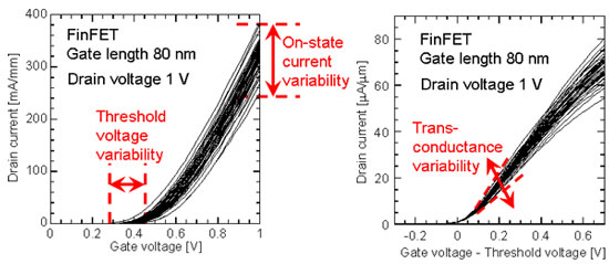 |
| Figure 2: Threshold voltage variability and trans-conductance variability that cause on-state current variability.
|
|
Based on the measured electrical characteristics, the researchers evaluated the variabilities of three parameters: threshold voltage, parasitic resistance, and trans-conductance. They analyzed in detail the correlations among the three parameters, the correlations between the on-state current and each of the parameters, and the correlations with the transistor-size variation. The contribution ratios of the three independent factors causing variability of on-state current were obtained and the trend of an increase in the on-state current variability due to a reduction in the transistor size was evaluated. The results revealed that although the contribution made by threshold voltage variability is reduced by thinning the gate insulators (AIST press release on June 15, 2010), variability of trans-conductance is difficult to reduce by miniaturizing the elements and will become an important factor as further element size reductions continue. It is predicted that variability of trans-conductance in the 14-nm-generation FinFETs is the dominant factor of on-state current variability (Fig. 3).
|
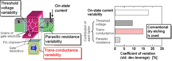 |
| Figure 3: Factors causing variability of on-state current in 14-nm-generation FinFETs (left) and the contribution of each factor (right).
|
|
The researchers also measured the trans-conductance variability in FETs with the fin channels formed by a conventional processing technique (dry-etching technique) and FETs formed by the nano-wet-etching technique developed at AIST. Figure 4 shows a Pelgrom plot of the measured variability of trans-conductance. The Pelgrom plot is used widely as an index of the variability of characteristics in transistors. The horizontal axis indicates the reciprocal of the square root of the gate area, whereas the vertical axis displays the coefficient of variation (standard deviation/mean value) of trans-conductance. The slope of plot, AGm, is the rate of increase in variability against the reduction in gate size; a smaller AGm value indicates better suppression of variability of characteristics. It was found that high-precision processing of silicon fin channels by the nano-wet-etching technique reduces the variability of trans-conductance.
|
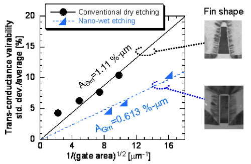 |
| Figure 4: Results of evaluations of trans-conductance variability.
|
|
Figure 5 shows the mechanism of the reduction in trans-conductance variability through the application of the nano-wet-etching technique. Further analysis of the possible factors causing trans-conductance variability revealed that the primary factor was the variability of mobility, which is determined by the scattering rate of carriers in the channels. Fin processing by the conventional dry-etching technique creates surface roughness of the fin sidewalls, reflecting the line-edge roughness of the resist. In addition, damage or charged defects can be produced by plasma in the fin channels during processing. These defects act as scattering centers of the carrier and reduce mobility. Conventional processing creates variation in the density of the scattering centers among transistors, consequently it causes variability of mobility. In contrast, applying the nano-wet-etching technique causes no damage to the fin channels, and the sides of the fins are extremely smooth. For these reasons, it is considered that the density of the scattering centers is kept low, suppressing mobility variability and the trans-conductance variability that it causes.
|
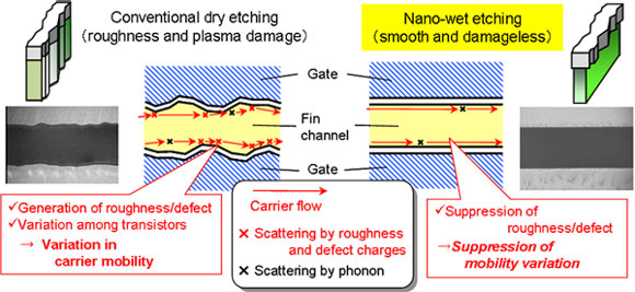 |
| Figure 5: Mechanism of reduction in trans-conductance variability by using the nano-wet-etching technique.
|
|
Predicted on-state current variability in 14-nm-generation FinFETs and the contribution of each major factor are shown in Fig. 6. When the fin channels are fabricated by a conventional dry-etching technique, trans-conductance variability is the dominant factor causing large variability of on-state current. However, processing the fin channels with high precision by the nano-wet-etching technique suppresses the trans-conductance variability to a low level and a reduction in on-state current variability is expected.
|
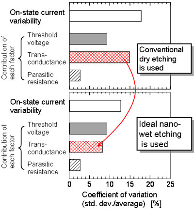 |
| Figure 6: Estimated contribution of each factor causing on-state current variability in 14-nm-generation FinFETs.
|
|
These results propose a solution to the variability issue of transistor characteristics that would be a serious concern in 14-nm-generation transistors. This solution would help to resolve the problem of reduced yields of integrated circuits such as SRAMs.
|
|
Future Plans
|
|
The researchers plan to fabricate integrated circuits using FinFETs aiming to demonstrate the improvements in yield and reliability at the circuit level.
|