| Mar 16, 2012 |
Novel 3D integration process flow: backside 'soft' via reveal
|
|
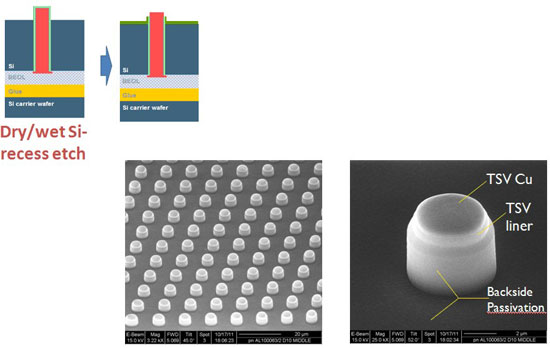
(Nanowerk News) Imec presents a via-middle through-Si-via (TSV) approach to 3D stacking. This method is new to industry as it allows to 'reveal' TSV contacts by using a Si-etch process. The process further allows thinning down the wafers to 50µm with a total thickness variation of less than 2µm.
|
|
In the new 3D integration flow, a TSV contact is buried in the wafer during front-side processing. After completion of the wafer processing, the wafer is thinned and the bottom side of the TSV contacts are 'revealed' in order to contact to a next layer of a 3D stack.
|
 |
| Wafers are thinned down to 50µm thickness, with a total thickness variation of less than 2µm.
|
|
This process is novel to IC manufacturing and has to be performed with great care, in order not to damage the devices. In the past year, great progress has been made with respect to the wafer-support system for handling 300mm wafers, thinned down to 50µm thickness. A total thickness variation (TTV) of the thinned wafer of less than 2µm has been achieved. Key step in this process is the bonding of the device wafer to a carrier wafer, prior to wafer thinning, by using a temporary adhesive. This material is stable during the subsequent process steps, but still allows for room temperature debonding of the thinned wafer upon completion of backside processing.
|
|
After wafer thinning, the backsides of the TSVs are successfully 'revealed' using a Si-etch process. Both wet and dry processes can be used. Chemical mechanical polishing (CMP) of the Cu/Si surface is not used as it results in a high risk of contamination and has a high cost-of-ownership. An effective via reveal process has been obtained using wet etching, exposing the TSVs uniformly on the wafer backside. In this stage, the TSV nails are still protected by their barrier and liner layers.
|
 |
| The 'soft' via reveal process with Si3N4 backside passivation.
|
|
The next step in the backside process consists of applying a backside passivation layer (this avoids Cu diffusion in the thin Si wafer) and selective opening of the liner layers on the TSV. This is achieved using a maskless, self-aligned dry etch-process.
|
|
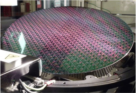
After this 'soft' via reveal process, further interconnect layers and bump interconnects can be processed on the wafer backside. The process is then completed by debonding the thin wafer from the carrier wafer and transferring the thin wafer to a dicing tape. This step can now be performed at room temperature. This process flow was successfully applied to a 300mm diameter wafer with active high-k/metal gate CMOS circuits.
|
|
|