| Mar 27, 2012 |
Researchers discover a new path for light through metal
|
|
(Nanowerk News) Helping bridge the gap between photonics and electronics, researchers from Purdue University have coaxed a thin film of titanium nitride into transporting plasmons, tiny electron excitations coupled to light that can direct and manipulate optical signals on the nanoscale. Titanium nitride's addition to the short list of surface-plasmon-supporting materials, formerly comprised only of metals, could point the way to a new class of optoelectronic devices with unprecedented speed and efficiency.
|
|
"We have found that titanium nitride is a promising candidate for an entirely new class of technologies based on plasmonics and metamaterials," said Alexandra Boltasseva, a researcher at Purdue and an author on a paper published today in the Optical Society's (OSA (http://www.osa.org)) open-access journal Optical Materials Express ("Titanium nitride as a plasmonic material for visible and near-infrared wavelengths"). "This is particularly compelling because surface plasmons resolve a basic mismatch between wavelength-scale optical devices and the much smaller components of integrated electronic circuits."
|
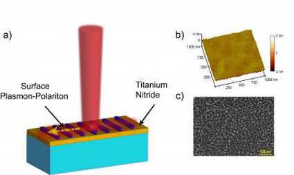 |
| This image shows a) Excitation by light of a surface plasmon-polariton on a thin film of titanium nitride. b) Atomic force microscope image of the surface of titanium nitride film. The mean roughness of the film is 0.5 nm. c) Scanning electron microscopy image of TiN thin film on sapphire. The texture shows multivariant epitaxial (crystalline) growth. (Image: Alexandra Boltasseva, Purdue University)
|
|
Value of Plasmons
|
|
Metals carry electricity with ease, but normally do nothing to transmit light waves. Surface plasmons, unusual light-coupled oscillations that form on the surface of metallic materials, are the exception to that rule. When excited on the surface of metals by light waves of specific frequencies, plasmons are able to retain that same frequency, but with wavelengths that are orders-of-magnitude smaller, cramming visible and near-infrared light into the realm of the nanoscale.
|
|
In the world of electronics and optics, that 100-fold contraction is a boon. Circuits that direct the paths of electrons operate on a much smaller scale than optical light waves, so engineers must either rely on small but relatively sluggish electrons for information processing or bulk up to accommodate the zippy photons. Plasmons represent the best of both worlds and are already at the heart of a number of optoelectronic devices. They have not had widespread use, however, due to the dearth of materials that readily generate them and the fact that metals, in most cases, cannot be integrated with semiconductor devices.
|
|
Plasmonic Materials
|
|
Until now, the best candidates for plasmonic materials were gold and silver. These noble metals, however, are not compatible with standard silicon manufacturing technologies, limiting their use in commercial products. Silver is the metal with the best optical and surface plasmon properties, but it forms grainy, or semi-continuous, thin films. Silver also easily degrades in air, which causes loss of optical signal, making it a less-attractive material in plasmon technologies.
|
|
In an effort to overcome these drawbacks, Boltasseva and her team chose to study titanium nitride—a ceramic material that is commonly used as a barrier metal in microelectronics and to coat metal surfaces such as medical implants or machine tooling parts—because they could manipulate its properties in the manufacturing process. It also could be easily integrated into silicon products, and grown crystal-by-crystal, forming highly uniform, ultrathin films—properties that metals do not share.
|
|
To test its plasmonic capabilities, the researchers deposited a very thin, very even film of titanium nitride on a sapphire surface. They were able to confirm that titanium nitride supported the propagation of surface plasmons almost as efficiently as gold. Silver, under perfect conditions, was still more efficient for plasmonic applications, but its acknowledged signal loss limited its practical applications.
|
|
To further improve the performance of titanium nitride, the researchers are now looking into a manufacturing method known as molecular beam epitaxy, which would enable them to grow the films and layered structures known as superlattices crystal-by-crystal.
|
|
Technologies and Potential Applications
|
|
In addition to plasmonics, the researchers also speculate that titanium nitride may have applications in metamaterials, which are engineered materials that can be tailored for almost any application because of their extraordinary response to electromagnetic, acoustic, and thermal waves. Recently proposed applications of metamaterials include invisibility cloaks, optical black holes, nanoscale optics, data storage, and quantum information processing.
|
|
The search for alternatives to noble metals with improved optical properties, easier fabrication and integration capabilities could ultimately lead to real-life applications for plasmonics and metamaterials.
|
|
"Plasmonics is an important technology for nanoscale optical circuits, sensing, and data storage because it can focus light down to nanoscale," notes Boltasseva. "Titanium nitride is a promising candidate in the near-infrared and visible wavelength ranges. Unlike gold and silver, titanium nitride is compatible with standard semiconductor manufacturing technology and provides many advantages in its nanofabrication and integration."
|
|
According to the researchers, titanium nitride-based devices could provide nearly the same performance for some plasmonic applications. While noble metals like silver would still be the best choice for specific applications like negative index metamaterials, titanium nitride could outperform noble metals in other metamaterial and transformation optics devices, such as those based on hyperbolic metamaterials.
|
|
|