| Apr 22, 2012 |
IBM demonstrates graphene devices for terahertz waves
|
|
(Nanowerk News) Graphene has been courted as the miracle material of the future, since different formulations have been fabricated into conductors, semiconductors and insulators. Now IBM has added photonic to the list by demonstrating a graphene/insulator superlattice that achieves a terahertz frequency notch filter and a linear polarizer, devices which could be useful in future mid- and far-infrared photonic devices, including detectors, modulators and three-dimensional metamaterials (see paper in Nature Nanotechnology: "Tunable infrared plasmonic devices using graphene/insulator stacks").
|
|
"In addition to its good electrical properties, graphene also has exceptional optical properties. In particular, it absorbs light from the far-infrared to to the ultra-violet," said IBM Fellow Phaedon Avouris. "The terahertz range was of particular interest to IBM, because these frequencies can penetrate paper, wood and other solid objects for security applications. Unfortunately, today there are very few ways of manipulating terahertz waves such as polarizing and filtering it, but because graphene operates well at terahertz frequencies we have concentrating on creating these types of devices."
|
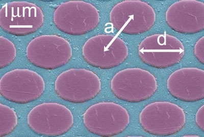 |
| Scanning Electron Microscope image of, five-layer graphene/insulator superlattice array of two-micron diameter microdisks (purple).
|
|
Teraherz frequency oscillations can be carried in graphene by plasmons—the collective oscillation of carriers—to enable low-loss tunable filters. But in single-layer graphene, the carrier concentration and resonant frequency was too weak for photonics applications, according to IBM. However, by going to a multi-layer graphene/instulator superlattice, transparent devices can be patterned into photonic-like crystals that distribute the carriers among the layers effectively enhancing both the carrier density and the resonant frequency.
|
|
"We have found that graphene interaction with electromagnetic radiation is particularly strong in the terahertz range, however with a single layer of graphene the interaction was still not strong enough," said Hugen Yan, a member of the Nanoscale Science and Technology Group at IBM's T. J. Watson Research Lab (Yorktown Heights, N.Y.) "But by using a multi-layer stack structure in microdisk arrays we achieved frequency selectivity in the terahertz range, allowing us to tune the desired resonant frequency."
|
|
IBM found that by patterning the graphene/insulator microdisks in arrays, it was able to tune their resonant frequency by varying the size of the microdisks, the number of layers, their spacing, and the doping of the graphene layers. Upon analysis, IBM discovered a unique carrier density scaling law for its graphene/insulator superlattices that, unlike conventional semiconductor superlattices, is based on laws governing Dirac fermions (such as quarks, leptons, baryons and hadrons).
|
|
As a result, IBM has been able to demonstrate patterned graphene/insulator stacks implementing a widely tunable notch filters with a 8.2-dB rejection ratio, and a terahertz linear polarizer with 9.5-dB extinction ratio. Implemented by laying down wafer scale alternating layers of graphene and a polymer insulator, then patterning them into microdisks, IBM demonstrated that these graphene/insulator superlattices shielded 97.5 percent of electromagnetic radiation at frequencies below 1.2 terahertz.
|
|
For the future, the research group intends to tune its graphene/insulator superlattices for the infrared frequencies used by optical communications equipment today. Fengnian Xia, a member of the Nanoscale Science and Technology Group at T. J. Watson Research Lab (Yorktown Heights, N.Y.), also contributed to the work.
|