| Jan 31, 2006 |
Novel nanotube positioning technique paves the way for integration into mass produced devices
|
|
(Nanowerk News) Researchers at UC Berkeley, led by Prof. Alex Zettl, have developed a combination of novel room temperature methods for both aligning and selectively
depositing nanotubes onto a topologically benign surface.
Using these methods, which can easily be integrated into
semiconductor manufacturing processes, they have fabricated
arrays of aligned torsional NEMS devices based on MWCNTs.
|
|
The research report "Controlled placement of highly aligned carbon nanotubes for the manufacture of arrays of nanoscale torsional actuators" was published in the Dec. 15, 2005 issue of Nanotechnology.
|
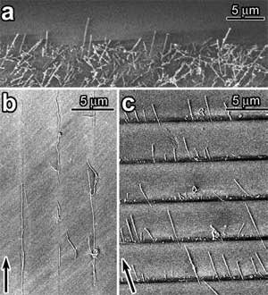 |
| Controlled deposition of nanotubes. (a) The edge of an unaligned mat of MWCNTs deposited on an area activated by the electron beam. The edge of the beam-activated area runs horizontally through the centre of the image. (b) SWCNTs placed by fluidic alignment onto beam activated lines which were oriented parallel to the direction of fluid flow. (c)MWCNTs placed by fluidic alignment at ∼70° to beam-activated lines. The arrows indicate the direction of flow. (Source: UC Berkeley)
|
|
Recent advances in nanoscale synthesis and fabrication
techniques have opened the door to the manufacture of
true nano-electromechanical systems (NEMS). For example,
multiwall carbon nanotubes (MWCNTs) have been utilized
as key enabling elements for nanoscale electrostatically
driven torsional and rotational actuators, orders
of magnitude smaller than their microelectromechanical
(MEMS) counterparts. Due to their small size, robust
design and near-perfect atomic structure, such constructs
hold great promise as building blocks for complex
nanoelectromechanical systems. The utility of individual
actuators can be significantly increased by their incorporation
into arrays of devices. Such arrays could serve in a variety
of applications, including adaptive optics, high frequency
mechanical filters, mass sensors, and microfluidic gates and
pumps.
|
|
A fundamental challenge in the development of NEMS
arrays (and of nanotube- and nanowire-based devices in
general) is the large-scale controlled placement of molecular
sized building blocks on a substrate. Methods based on
chemical vapour deposition (CVD) avoid this problem by,
for example, growing nanotubes directly on the substrate
where they ultimately will be located. Unfortunately,
such methods are unable to produce very high quality
multi-walled carbon nanotubes as are often required for NEMS applications. Furthermore, CVD is commonly a high temperature process, which severely
limits compatibility with substrate materials or other system
components. Hence there is much interest in low temperature
techniques to aid in the selective placement and alignment of
prefabricated nanostructures. There has been some progress
in developing fluidic techniques for aligning nanowires
and nanotubes, and various functionalization schemes
have been explored for placing nanotubes on particular areas
of a substrate. Unfortunately, most of these methods
necessitate rather complex substrate topology or involved and
limiting chemistry.
|
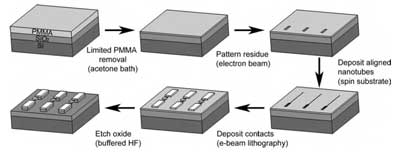 |
| Fabrication process. A silicon/silicon oxide wafer is coated with electron beam resist (not to scale) which is then mostly removed in an acetone bath. The remaining residue is then patterned by exposure to an electron beam in situ in an SEM. MWCNTs are deposited out of solution onto the spinning substrate, causing them to align with fluid flow and adhere to the exposed pattern. Standard electron beam lithography is then used to deposit anchors and paddles. Finally, the silicon oxide is partially etched down to suspend the nanotube–paddle assemblies. (Source: UC Berkeley)
|
|
In summary, the researchers have fabricated arrays of torsional actuators
using a novel nanotube positioning technique. The nanotubes
are oriented by fluid flowacross a spinning substrate and adhere
preferentially to regions that have been activated by a focused
electron beam. The adhesion is found to be due to extreme
modification of a residual polymer layer already present in
lithographic work. By varying the flow direction and electron
beam exposure we are able to deposit nanotubes in a variety
of patterns that can then be contacted by standard lithography.
Our ability to orient and preferentially place molecular
structures paves the way for their integration into mass
produced devices. Aside from the torsional actuator array
already described, an immediate, simple application is the
use of nanotubes as electrical interconnects between units
of an integrated circuit (especially desirable due to their
ability to carry extremely high electrical and thermal current
densities). The unique physical properties of carbon nanotubes
could be harnessed in other applications as well, such as
high density arrays of field effect transistors, gas sensors or
biosensors. Alternative geometrical configurations, including
radially aligned nanotubes, crossed nanotubes etc, could be
easily fabricated using the techniques described here.
|