| May 23, 2012 |
Researchers improve infrared detectors using single-walled carbon nanotubes
|
|
(Nanowerk News) Whether used in telescopes or optoelectronic communications, infrared detectors must be continuously cooled to avoid being overwhelmed by stray thermal radiation. Now, a team of researchers from Peking University, the Chinese Academy of Sciences, and Duke University (USA) is harnessing the remarkable properties of single-walled carbon nanotubes (SWNTs) to create highly sensitive, "uncooled" photovoltaic infrared detectors.
|
|
This new type of detector, which the team describes in a paper published today in the Optical Society's (OSA) open-access journal Optical Materials Express ("Carbon nanotube arrays based high-performance infrared photodetector"), may prove useful for industrial, military, manufacturing, optical communications, and scientific applications.
|
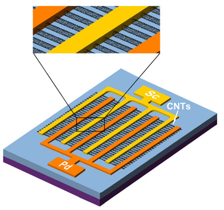 |
| This schematic shows the design of single-walled carbon nanotube photodetector, which provides a more efficient method of collecting infrared radiation without relying on cryogenics for cooling. (Image courtesy Sheng Wang, Peking University)
|
|
Carbon nanotubes are known for their outstanding mechanical, electrical, and optical properties. "They also are an ideal nanomaterial for infrared applications," says Sheng Wang, an associate professor in the Department of Electronics at Peking University in Beijing, China, and an author of the Optical Materials Express paper. "For starters, these nanotubes exhibit strong and broadband infrared light absorption, which can be tuned by selecting nanotubes of different diameters. Also, due to their high electron mobility, nanotubes react very rapidly – on the order of picoseconds – to infrared light." In comparison to traditional infrared detectors, which are based on semiconductors made of a mercury-cadmium-telluride alloy, the SWNTs are an order of magnitude more efficient, the researchers report.
|
|
The team's photovoltaic infrared detector is formed by aligning SWNT arrays on a silicon substrate. The nanotubes arrays are then placed between asymmetric palladium and scandium contacts. These two metals have properties that collectively create what is known as an Ohmic contact, a region in a semiconductor device that has very low electrical resistance, which helps make the detector operate more efficiently.
|
|
"Fabrication of carbon nanotube infrared detectors can be readily implemented on a flexible substrate and large wafer at a low cost," explains Wang.
|
|
The detector demonstrated "acceptable sensitivity" at room temperature and may be significantly improved by increasing the density of the carbon nanotubes, according to the team. The signal-to-noise performance of conventional infrared photodetectors is limited by their natural infrared emission, which is subsequently absorbed by the detector. To avoid having this stray radiation overwhelm the detector, liquid nitrogen or electric cooling is generally used to suppress this thermal effect. However, this makes infrared detectors more complex and expensive to operate. The new design eliminates this need because carbon nanotubes have special thermal properties. At room temperature, they emit comparatively little infrared radiation of their own, especially when the carbon nanotube is on the substrate. In addition, nanotubes are very good at conducting heat, so temperatures do not build up on the detector itself.
|
|
One of the biggest surprises for the team was achieving relatively high infrared detectivity (the radiation power required to produce a signal from a photoconductor) using a carbon nanotube thin film only a few nanometers thick, Wang points out. Notably, conventional infrared detectors require much thicker films, on the scale of hundreds of nanometers, to obtain comparable detectivity.
|
|
Another huge advantage of the detector is that the fabrication process is completely compatible with carbon nanotube transistors – meaning no big expensive equipment changes are necessary. "Our doping-free chemical approach provides an ideal platform for carbon nanotube electronic and optoelectronic integrated circuits," says Wang.
|
|
The next step for the team is to focus on improving the detectivity of the detector with greater SWNT density, and to also achieve a wide spectrum response with improved diameter control.
|