| Jun 11, 2012 |
Small worlds come into focus with new Sandia instrument
|
|
(Nanowerk News) Paul Kotula recently told a colleague at another laboratory that Sandia's new aberration-corrected scanning transmission electron microscope (AC-STEM) was like a Lamborghini with James Bond features.
|
|
The $3.2 million FEI Titan G2 8200 Sandia accepted in February is 50 to 100 times better than what went before in terms of resolution and the time it takes to analyze a sample, say Paul and Ping Lu (both 1822), principal investigators.
|
|
Its unique combination of X-ray detectors and very high resolution offers magnification that Paul compares to a telescope powerful enough to show two peas side by side on the moon. Slides of microstructures analyzed with the AC-STEM and Sandia's older analytical microscope highlight the new capabilities, with a clear image from the AC-STEM and a fuzzy one from its predecessor. An analysis that took seven minutes on the AC-STEM took two hours on the previous instrument, he says.
|
|
Ping and Paul operate the microscope from a basement lab adjacent to the environment-controlled room that houses it. They're not in the same room because the instrument is so sensitive even clicking a computer mouse against a desk would cause an image to jump, Ping says.
|
|
"At the atomic scale, it doesn't take too much," he says.
|
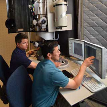 |
| Principal investigators Paul Kotula, left, and Ping Lu show off Sandia's new aberration-corrected scanning transmission electron microscope, which has a unique combination of X-ray detectors and very high resolution and is capable of doing analyses in far less time than the Labs' older analytic microscope.
|
|
Operating unit from 1,000 miles away
|
|
The remote operation affords another advantage: Sandia/California researchers can run it from 1,000 miles away, which they demonstrated in March. Paul jokes the only thing they can't do from California is load the sample and fill the liquid nitrogen that cools the machine.
|
|
The AC-STEM delivers electron beams accelerated at voltages from 80 kV to 200 kV, allowing researchers to study properties of structures at the nanoscale — very important for materials science in everything from microelectronics to nuclear weapons.
|
|
The physics of nanomaterials are different, Paul and Ping say.
|
|
"They have different optical properties than bulk material — gold nanoparticles versus gold foil, they're totally different," Paul says.
|
|
Any impurities or structural defects hurt performance in super thin microelectronics layers, for example, he says. In the same way, interfaces in a weapon are critical because that's where any impurities tend to be, "where you might get some sort of separation or corrosion or reaction happening that's the basis of aging of these materials," he says. "Being sensitive to that lets us help others predict lifetimes, replacement intervals, or failure modes so we know what to look for."
|
|
It takes powerful instruments to do those studies.
|
|
"You need this kind of tool to quantify it," says Ping as he sits in front of a computer screen showing an image of a 50-nanometer-thick specimen inside the AC-STEM — a sample 2,000 times thinner than the thickness of a human hair.
|
|
What looks like a close-up of mesh or lattice on the screen is really an image of 3-angstrom atomic spacing between titanium and strontium. An angstrom equals one 10th of a billionth of a meter.
|
|
The microscope uses a unique in-lens design in which four X-ray detectors surround a sample placed in the center, increasing collection efficiency, Ping says.
|
|
Older instruments were limited by lens aberrations, particularly spherical aberration that prevents sharp focus because electrons off of the optical axis are focused more strongly than ones near the optical axis, Paul says. The AC-STEM's additional lenses and computational elements negate that, he says.
|
|
"With the aberration-correction technology, you can open the aperture up and keep all those electrons focused to a nice point on your sample," he says.
|
|
Atomic resolution requires a tiny probe and scanning the sample at very high magnification.
|
|
Preventing damage to samples
|
|
The AC-STEM can put the probe on a sample for tens of microseconds or even milliseconds and gather enough information for researchers to tell what elements are present at atomic resolutions, Paul says. The probe returns to the same spot repeatedly with a drift correction that prevents a blurred image, collecting a stream of X-ray photons while minimizing damage since short duration equals a smaller dose rate.
|
|
High electron beam currents can damage some samples. However, "you can easily back off on the intensity" of the AC-STEM's beam because it has so many adjustable parameters, Paul says.
|
|
A dark spot that looks like a hole in Ping's sample indicates damage, but it's deliberate as he sputters atoms from the sample with a 200kV electron beam, knocking atoms out of the lattice to measure how removing part of the sample affects the X-ray signal.
|
|
The AC-STEM also studies material in the micron world. Although a hundred microns is about the smallest size a human eye can see, it's a huge scale for a transmission electron microscope.
|
|
At the micron level, "we're not making such a fine beam anymore but we're using the collection efficiency and the bright electron source to be able to be sensitive to small concentrations," Paul says. "That's very important for a lot of our customers who are looking for impurities in some of these materials."
|
|
First commercial unit fielded
|
|
The room that houses the microscope has to remain stable in terms of vibration, acoustics, temperature, and electromagnetic fields. Acoustic and chilled water panels line the walls, and the room's 65-degree temperature varies less than a tenth of a degree Celsius over half an hour. The instrument's accelerator, capable of producing 200,000 volts, is stowed behind acoustic drapes in a corner to isolate vibrations from the 9.5-foot-tall column containing various types of lenses and the instrument's in-lens X-ray detectors.
|
|
Sandia's AC-STEM is the first commercial unit fielded, based in part on development funded by a DOE Basic Energy Sciences project aimed at developing advanced electron microscopes built around aberration-correcting optics. The Transmission Electron Aberration-corrected Microscope, or TEAM project, was a collaboration involving the Argonne, Brookhaven, Lawrence Berkeley, and Oak Ridge national laboratories and Frederick Seitz Materials Research Laboratory.
|
|
The concept was theorized in the 1950s but computers were in their infancy and no one could manually adjust microscopes requiring multiple alignments and mechanical and power stability, Paul says.
|
|
"This new transmission electron microscope is now the flagship of our departmental capabilities that include professionally maintained, state-of-the-art equipment in all types of bulk material analysis — gas, liquid, solid — and microstructural characterization, including electron optics, diffraction, and spectroscopy," says manager Jim Aubert.
|
|
The AC-STEM offers endless potential for collaboration with colleagues in the Labs and at other national laboratories, companies, and universities since they don't have to be on site to participate, the researchers say
|
|
"Other colleagues can go online and look over your shoulder virtually," Paul says.
|