| Apr 04, 2006 |
Successful development of a desktop apparatus enabling nanometer-scale fabrication
|
|
(Nanowerk News) The National Institute of Advanced Industrial Science and Technology (AIST) in Japan has succeeded in the development of a nano-fabrication technique utilizing a thermal lithography method resulting from the combination of visible-light lithography using a semi-conductor laser with a thermally nonlinear material. By combining the thermal lithography technique of AIST with optical disc-related techniques of Pulstec Industrial Co. Ltd., a nano-fabrication apparatus has been developed.
|
|
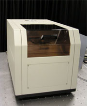
The apparatus AIST has developed enables the formation of 50 nm-fine structures over a wide area of 12 cm in diameter, the size of an optical disc, at high-speed. It is easy to handle because of its desktop size, and its price is one fourth of the corresponding conventional ones.
|
  |
|
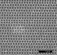
Left: The jointly-developed desktop nano-fabrication apparatus. Right: An example of a nano-pattern drawn by the apparatus (Source: AIST)
|
|
The apparatus is easily handled by anyone, and enables nanometer-scale fabrication at low cost, which until now could only be done with expensive large apparatus using short wavelength light, such as vacuum ultraviolet light (for the photolithography method) and electron beams (for the electron beam lithography method). Our technique is expected to facilitate reduction in the cost of optical devices with fine structures, e.g., photonic crystals and antireflective structures, and to be applied to nanotechnologies.
|
|
This work was presented at the 53rd Spring Meeting, 2006 The Japan Society of Applied Physics on March 22-26 at Musashi Institute of Technology.
|