| Apr 07, 2006 |
Success in real-ime observation of nanoscale cutting process
|
|
(Nanowerk News) The National Institute of Advanced Industrial Science and Technology (AIST) and Toyama University in Japan have jointly developed a nano-mechanical fabrication system working in a scanning electron microscope (SEM), and thereby succeeded in real-time imaging of the nano-scale cutting process for a single crystal of silicon.
|
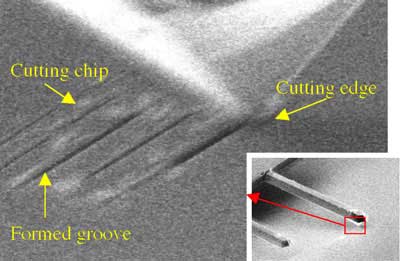 |
A SEM image of the nano-cutting process (captured from movie) (Source: AIST)
|
|
The fabrication system we have developed utilizes the mechanics of atomic force microscopes (AFM), in which we use a special cantilever for fabrication which has been developed by ourselves. For nano-scale cutting in this system, the cutting depth can be controlled in the range of 1-100 nm by changing the normal load applied to the cutting edge fixed on the cantilever tip. The tip of the cutting edge can be observed by SEM, and thereby the nano-scale cutting process can be recorded as a movie.
|
|
The direct observation of the fabrication process can provide more valuable information than point signal logging, and can thus be a powerful tool for clarifying the removal mechanism of materials by cutting and for determining optimal fabrication conditions. The developed nano-fabrication system operating in SEM is expected to accelerate development of the practical use of nano-fabrication techniques, e.g. fabrication and repair of nano-molds etc. used in nano-imprints.
|