| Posted: March 25, 2008 |
Nanoelectronics : the compression of light directly observed by researchers |
|
(Nanowerk News) A team of researchers from CEA (Institut rayonnement matière Saclay) and the Université de Technologie de Troyes associated with CNRS (Institut Charles Delaunay) has observed, through a microscope, plasmons on the surface of conductors measuring 30 nanometers. The use of such plasmons, signals that are at the limit of electronics and optics, is becoming, on this scale, an important issue for the much sought-after miniaturization of electronic circuits.
|
|
This is the first time that images of such high resolution have been obtained for these phenomena, which have been studied for the last ten or so years. This observation is the subject of an article published in Nano Letters dated 12 March 2008.
|
|
In electronics, there is continuing technological effort to produce smaller and smaller circuits capable of processing information at higher and higher frequencies. Although electronic devices are becoming both more compact and more complex (computer micro-processors), they are still limited to the usual frequencies of about a gigahertz. Optical frequencies are one million times higher (1015 Hz), but the spatial limits imposed by the wavelength of light (around one micron) prevent further miniaturization.
|
|
To reduce the wavelength further and, as it were, compress light, one solution consists in converting the light signal into a plasmon. The plasmon is a phenomenon that has all the characteristics of a light wave, except that it remains confined within the walls of a metal conductor. When the diameter of the metal object is reduced to 30 nm, the plasmon develops a mode known as “slow” (referred to as slow plasmon mode). However, this slow mode has the property of oscillating at the frequency of the light wave while possessing a wavelength well below that of light.
|
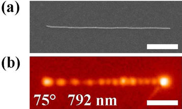 |
| Fig. 1: a) 30 nm diameter and 4 µm long gold wire. b) PEEM observation of the signal of electrons emitted showing the interference between the incident light and the plasmon, which propagates along the wire. (Image: CNRS)
|
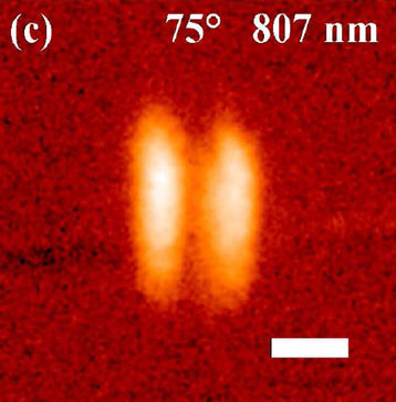 |
| Fig.2: PEEM observation of the excitation of the plasmon mode of a 100 mm long rod by light at 807 nm. (Image: CNRS)
|
|
Researchers are interested in this slow plasmon mode because it is on this same scale, approaching 30 nm, that the limits of miniaturization in electronics will soon be set.
|
|
Although the principles were already known, they had not yet been experimentally observed. When a plasmon excited by light propagates along a conductor, different secondary effects appear, including the emission of electrons. The researchers therefore used a PEEM (Photo Emission Electron Microscopy) microscope to obtain these images.
|
|
The first figure shows the emission from a gold wire. The intensity modulations result from the interference between the slow plasmon and the excitation light wave.
|
|
The very high resolution image (fig.2) shows a slow plasmon excitation mode of a 100 nm long “rod” by light with a wavelength of 807 nm. The wavelength compared to the wavelength of light (between 250 and 300 nm) may here be compressed threefold.
|
|
By converting the information from an optical signal to a slow plasmon, it is therefore possible to envisage, for structures close to 30 nm, reconciling high optical frequencies with the “classical” dimensions of silicon electronics.
|