| Posted: April 22, 2008 |
An organizer for structuring silicon |
|
(Nanowerk News) Organizers make life easier; aluminum could help the semi-conductor industry to convert silicon from a disordered to an ordered form at low temperatures. This crystalline silicon functions much more efficiently in solar cells, for example. However up to now it has only been possible to manufacture it at high temperatures and it could therefore not be applied to heat-sensitive materials such as plastic or paper.
|
|
Scientists at the Max Planck Institute for Metals Research in Stuttgart have now found a way to systematically lower the crystallization temperature of silicon - from 700° to 150°Celsius and to any temperature within that range. They succeeded in doing this by applying a thin layer of aluminum to disordered silicon; the thickness of the layer determined the crystallization temperature. The researchers have also explained why this happens. These findings could help to manufacture solar cells and other electronic components on cheap and flexible materials such as glass, plastic or even paper (" Tailoring the Ultrathin Al-Induced Crystallization Temperature of Amorphous Si by Application of Interface Thermodynamics").
|
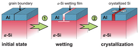 |
| Atomic ordering in the gap: a covering layer of aluminum lowers the crystallization temperature of amorphous silicon (a-Si). First the a-Si covers ("wets") the grain boundaries in the aluminum layer (A1). Once the wetting a-Si film has reached a critical thickness, crystallization starts at the grain boundaries. (Image: Max Planck Institute of Metals Research)
|
|
Silicon is the material of choice in the semi-conductor industry. Sometimes it needs to be in a crystalline form and sometimes in an amorphous, that is, a disordered form. Because the range of applications for chips and solar cells is so wide, the materials which act as carriers of the semi-conductor and the conditions under which they have to work, have become correspondingly varied. The industry would therefore like to be able to deliberately manipulate the temperature at which silicon crystallizes. Mostly, they want to lower the temperature, so that they can get the semi-conductor material to crystallize on heat-sensitive materials. Sometimes, however, they also want to prevent the silicon from changing from the amorphous to the crystalline form.
|
|
It has long been known that the crystallization temperature of a semi-conductor changes when it is in contact with a different metal. "We have exploited this effect for the first time in order to set the crystallization temperature of silicon using a covering layer of aluminum crystals," says Lars Jeurgens, one of the researchers in Eric J. Mittemeijer’s department at the Max Planck Institute of Metals Research in Stuttgart who was involved. It is possible to get it below 200° with layers thicker than 20 nanometers. With thinner layers, the temperature rises considerably.
|
|
The scientists in Stuttgart were only able to control the temperature so precisely because they had clarified in advance what the effect was based on and how it could be described theoretically. It was already known that the aluminum layer weakens the bonds between the silicon atoms. It is therefore easier for them to rearrange themselves in an ordered form which has the effect of lowering the energy of the silicon block. If there is no aluminum layer to loosen the bonds in the amorphous silicon, a temperature of 700° Celsius is required to break them up.
|
|
The extent to which the thickness of the aluminum layer lowers the crystallization temperature depends on the variations of energy contributions in the system formed by the silicon block and the aluminum layer. The maxim is: everything is done to save energy. The energies at the interface between the silicon and the aluminum play a major role. In order to lower the total energy of the system, the silicon atoms first position themselves in a disordered way at the aluminum grain boundaries. It is easier for them to adapt to the crystal lattice of the aluminum if they are in a disordered state. If they were to order themselves there would be energy-consuming tensions at the boundary between the two different and rigid crystal lattices.
|
|
Although it initially does not sound like it, this encourages the silicon to crystallize - albeit indirectly. As soon as a thin, disordered silicon layer has formed on the aluminum grain boundary, there is another opportunity to save energy: the silicon atoms arrange themselves neatly into a crystal. The crystallization energy and the change of interface energy are decisive here, because they determine the temperature at which the covering silicon layer starts to crystallize. The researchers in Stuttgart manipulate this fine balance deliberately by varying the thickness of the aluminum layer.
|
|
In these studies, the researchers initially concentrated on the moment at which crystallization starts. What happens afterwards has not yet been completely explained. During the process, crystalline silicon gradually displaces the aluminum layer. The aluminum atoms travel through the crystalline silicon and collect at the bottom of the silicon block. Why they do this and what exactly happens is now being examined by the materials scientists in Eric. J. Mittemeijer’s department.
|