| Aug 28, 2008 |
University of Washington buys multimillion-dollar tool for nanotechnology research
|
|
(Nanowerk News) The University of Washington will acquire an electron beam lithography machine, a key instrument required to build devices at the nanometer scale. A $1.3 million gift from the Washington Research Foundation provides about half the cost of the $2.5 million electron beam lithography machine, which will be the only one of its kind in the Northwest.
|
|
"The electron beam lithography machine will give researchers at the University of Washington the ability to work on nanoscale projects with a broad range of possible commercial applications," said Ron Howell, CEO of the Washington Research Foundation. "This tool will place the university among a handful of institutions with such a capability. Ultimately, it could lead to the creation of many new companies and products."
|
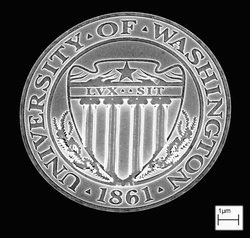 |
| An etching of the UW seal made using an electron beam lithography machine at Cornell University. Around 100 of these seals would fit on the end of a human hair.
|
|
The Washington Research Foundation was created in 1981 to support research and entrepreneurship at state research institutions. The gift is among the largest gifts in its history.
|
|
Nanoscale devices have promising commercial potential for solar cell materials, new displays, memory chips, photonic devices and biological sensors, among many other applications.
|
|
"Our region has the capacity for being a serious player in nanoscience. This is a key piece that will allow Pacific Northwest researchers to compete in this field in the international arena," said Matt O'Donnell, dean of the College of Engineering.
|
|
The remaining $1.2 million of the machine's cost will come from the UW through the Innovative Research Teams fund, a state program created by the Economic Development Commission to recruit researchers in areas that have the potential for significant economic impact.
|
|
The electron beam lithography machine works by scanning a beam of electrons across a surface to sketch small-scale patterns that can be used in circuits or other devices. In the commercial processes used to build computer chips, light is generally used instead of an electron beam -- which is ideal for large-scale device production, but is not as flexible or precise as using electron beams. An electron beam lithography tool like this one can draw devices down to about 10-nanometer resolution on surfaces up to eight inches wide. The device can also be used to build 3-D structures by building multiple layers. A nanometer is a unit of measurement equal to one billionth of a meter.
|
|
The UW's portion was part of a recruitment package for Michael Hochberg, an assistant professor of electrical engineering, who arrived at the UW from the California Institute of Technology in 2007.
|
|
Hochberg's research is in nanophotonics, a field that uses light photons rather than electrons to transmit and process information. Using photons allows the possibility of creating tiny chips that use less power and transmit information more quickly than current electronic devices. Hochberg's lab members are expected to be major users for the new machine.
|
|
"This is the most flexible, capable machine that you would buy to build nanostructures," Hochberg said. "This is a prototyping machine -- the kind of system used to prototype technologies that are still five, 10 or 20 years out."
Other local researchers have already expressed interest. About 30 UW faculty members said they will make use of the device, including members of the departments of physics, electrical engineering, bioengineering and chemistry. Researchers at a number of local companies have expressed a strong interest in using the machine, which will be housed in Fluke Hall at the Washington Technology Center clean room, a state-funded micro- and nano-fabrication facility on the UW campus.
|
|
The machine should be installed within a year and will be available at a fee for use by those inside and outside the UW doing nanotechnology research.
|
|
|