| Posted: October 13, 2008 |
IMEC demonstrates 3D stacked integrated circuits |
|
(Nanowerk News) IMEC, Europe’s leading independent nanoelectronics research institute today announced that it has made significant progress with its 3D-SIC (3D stacked IC) technology. IMEC recently demonstrated the first functional 3D integrated circuits obtained by die-to-die stacking using 5µm Cu through-silicon vias (TSV). It will now further develop 3D SIC chips on 200mm and 300mm wafers, integrating test circuits from partners participating in its 3D integration research program.
|
|
IMEC reported a first-time demonstration of 3D integrated circuits obtained by die-to-die stacking and using 5µm Cu through-silicon vias (TSV). The dies were realized on 200mm wafers in IMEC’s reference 0.13µm CMOS process with an added Cu-TSVs process. For stacking, the top die was thinned down to 25µm and bonded to the landing die by Cu-Cu thermocompression. IMEC is upscaling the process for die-to-wafer bonding and is on track for migrating the process to its 300mm platform.
|
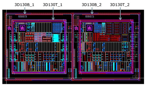 |
| Test-chip taped for assessing design rules and models for 3D-SIC technology.
|
|
To evaluate the impact of the 3D SIC flow on the characteristics of the stacked layers, both the top and landing wafers contained CMOS circuits. Extensive tests confirmed that the performance of the circuits does not degrade with adding Cu TSVs and stacking. And to test the integrity and performance of the 3D stack, ring oscillators with varying configurations were made, distributed over the two chip layers and connected with the Cu TSVs. Tested after the TSV and stacking process, these circuits demonstrated the chips excellent integrity.
|
|
“With these tests, we have demonstrated that our technology allows designing and fabricating fully functional 3D SIC chips. We are now ready to accept reference test circuits from our industry partners,” commented Eric Beyne, IMEC Scientific Director for 3D Technologies, “This will enable the industry to gain early insight and experience with 3D SIC design, using their own designs”.
|
|
About IMEC
|
|
IMEC is a world-leading independent research center in nanoelectronics and nanotechnology. IMEC vzw is headquartered in Leuven, Belgium, has a sister company in the Netherlands, IMEC-NL, offices in the US, China and Taiwan, and representatives in Japan. Its staff of more than 1600 people includes more than 500 industrial residents and guest researchers.
|
|
IMEC’s More Moore research aims at semiconductor scaling towards sub-32nm nodes. With its More than Moore research, IMEC looks into technologies for nomadic embedded systems, wireless autonomous transducer solutions, biomedical electronics, photovoltaics, organic electronics and GaN power electronics.
|
|
IMEC’s research bridges the gap between fundamental research at universities and technology development in industry. Its unique balance of processing and system know-how, intellectual property portfolio, state-of-the-art infrastructure and its strong network worldwide position IMEC as a key partner for shaping technologies for future systems.
|
|
Further information on IMEC can be found at www.imec.be.
|