| Posted: November 10, 2008 |
Novel method can mass produce graphene |
|
(Nanowerk News) Graphene is a perfect example of the wonders of nanotechnology, in which common substances are scaled down to an atomic level to uncover new and exciting possibilities.
|
|
Graphene is created when graphite — the mother form of all graphitic carbon, which is used to make the pigment that allows pencils to write on paper — is reduced down to a one-atom-thick sheet. Graphene is among the strongest materials known and has an attractive array of benefits. These sheets — single-layer graphene — have potential as electrodes for solar cells, for use in sensors, as the anode electrode material in lithium batteries and as efficient zero-band-gap semiconductors.
|
|
Research on graphene sheets has been restricted, though, due to the difficulty of creating single-layer samples for use in experiments. But in a study published online Nov. 9 in the journal Nature Nanotechnology, researchers from UCLA's California NanoSystems Institute (CNSI) propose a method which can produce graphene sheets in large quantities.
|
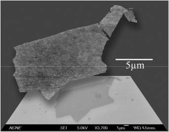 |
| Two overlapping images of the same graphene sheet produced by hydrazine reduction; the top image was produced using atomic force microscopy, while the bottom was produced with scanning electron microscopy. This is the first reported instance of a graphene sheet being large enough for both tests to be run on the same specimen. (Image: Vincent Tung, Matthew Allen, Adam Stieg)
|
|
Led by Yang Yang, a professor of materials science and engineering at the UCLA Henry Samueli School of Engineering, and Richard Kaner, a UCLA professor of chemistry and biochemistry, the researchers developed a method of placing graphite oxide paper in a solution of pure hydrazine (a chemical compound of nitrogen and hydrogen), which reduces the graphite oxide paper into single-layer graphene.
|
|
Such methods have been studied by others, but this is the first reported instance of using hydrazine as the solvent. The graphene produced from the hydrazine solution is also a more efficient electrical conductor. Field-effect devices display output currents three orders of magnitude higher than previously reported using chemically produced graphene. Kaner and Kang's co-authors on the research were doctoral students Vincent Tung, from Yang's lab, and Matthew Allen, from Kaner's lab.
|
|
"We have discovered a route toward solution processing of large-scale graphene sheets," Tung said. "These breakthroughs represent the future of graphene nanoelectronic research."
|
|
The coverage of the graphene sheets can be controlled by altering the concentration and composition of the hydrazine solution. This hydrazine method also preserves the integrity of the sheets, producing the largest-area graphene sheet yet reported, 20 micrometers by 40 micrometers. A micrometer is one-millionth of a meter, while a nanometer is one billionth of a meter.
|
|
"These graphene sheets are by far the largest produced, and the method allows great control over deposition," Allen said. "Chemically converted graphene can now be studied in depth through a variety of electronic tests and microscopic techniques not previously possible."
|
|
"Interdisciplinary research of this sort is a benefit of collaborative institutes like the CNSI," said Kaner, who is also an associate director of the CNSI. "Graphene is a cutting-edge nanomaterial and one which has great potential to revolutionize electronics and many other fields."
|
|
There are two methods currently used for graphene production — the drawing method and the reduction method, each with its own drawbacks. In the drawing method, layers are peeled off of graphite crystals until one is produced that is only one-atom thick. When likely graphene suspects are identified from the peeled layers, they must be extensively studied to conclusively prove their identity. In the reduction method, silicon carbide is heated to high temperatures (1100° C) to reduce it to graphene. This process produces a small sample size and is unlikely to be compatible with fabrication techniques for most electronic applications.
|
|
"This technology (hydrazine reduction) utilizes a true solution process for graphene, which can dramatically simplify preparing electronic devices," said Yang, who is also faculty director of the Nano Renewable Energy Center at the CNSI. "It thus holds great promise for future large-area, flexible electronics."
|