| Posted: January 23, 2009 |
New nano-simulation tools to design smaller transistors |
|
(Nanowerk News) The semiconductor industry is in peril, experts say.
|
|
As chips get smaller and smaller, they grow intensely hot, power-hungry and unreliable. Furthermore, at the nano-regime (10 nanometers and smaller; 5,000 times thinner than a strand of hair), the electrons that flow through semiconductors begin to behave like waves, ruled by the laws of quantum mechanics, and chips lose their efficiency.
|
|
“The semiconductor industry is going to come to a halt in ten years unless we find design alternatives,” said Gerhard Klimeck, a professor of electrical and computer engineering at Purdue University and associate director for technology at the Network for Computational Nanotechnology (NCN). “We must get away from traditional designs which are, in a sense, one-dimensional, modified layer by layer, and start modifying devices to vary on a three-dimensional scale. For that, we need a different simulation engine.”
|
|
Such a simulator would have to take into account both the quantum behavior and the atomic-level detail of their components, which makes them far more complex to model than today’s chips.
|
|
Klimeck is both a designer of nanoelectronic components — quantum dots, wires and wells — and the creator of some of the most effective tools for the design of these next-generation parts.
|
|
Working first at Texas Instruments, then the NASA Jet Propulsion Laboratory, and now at Purdue’s Network for Computational Nanotechnology, Klimeck has been at the cutting edge of computational semiconductor simulation, producing tools that enable thousands of scientists to understand and design ever-shrinking electronics.
|
|
What will these future devices look like? How will they be designed and manufactured? And how can they be optimized quickly to keep the semiconductor industry on track?
|
|
The answers to these questions have major ramifications, not just for the ubiquitous computer industry, but also for detectors, lasers, and green energy solutions, all of which will impact our lives.
|
|
The Growth of the Simulator
|
|
In the early 1990s, Klimeck began working on the first incarnation of a simulation engine that could predict how miniaturized semiconductors would behave. “NEMO 1D” delivered atomistic, quantum transport simulations, modeling how electrons would act in the first room temperature, quantum effect logic and memory device: the resonance tunneling diode.
|
|
However, NEMO 1D could only represent the diode in one dimension, and thus simplified many aspects of the device’s behavior. In its time, it was radical, and it remains a useful tool for designers today. But Klimeck knew that he had to set his sights higher to achieve his long-term goal of sustainable nano-electronic design.
|
|
He began work on NEMO 3D knowing that the calculations required to solve the three-dimensional transport equations were then intractable. “In 1998, it was completely unfeasible to think about quantum transport — taking an electron on one side and pulling it out on the other side of the device,” Klimeck said. “What was feasible, however, was to look at a million atom electronic structure, i.e. looking at the states where electrons could reside, without the transport component.”
|
|
But as the speed and memory of computers increased exponentially over the last decade, what was at first only geared towards quantum dots grew into a useful tool for the simulation of small-scale systems generally.
|
|
“Now, you can look at single impurities on semiconductors and at electronic states on nanowires and quantum wells in a three-dimensional representation where you can place one atom at a time, and replace it with others, and see what effect the disorder has on the system,” Klimeck said.
|
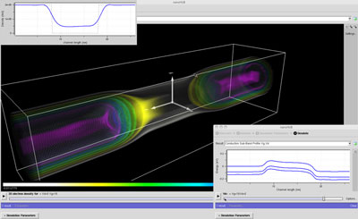 |
| Full 3D Volume Rendering of Electrostatic Potentials and Electron Densities: The nanoVIS technology integrated into the Rappture and nanoHUB middleware allows developers to deploy tools that provide rapid and fully integrated volume rendering of 3D data. This is a screen shot taken from an animation of the nanowire tool which illustrates the development of the electron charge and the electrostatic potential inside a circular nanowire.
|
|
Work based on NEMO3D explaining the experimental effects of single impurities in advanced nano finFETs has recently been published in Nature Physics and the prestigious Electrical Engineering Device Conference at IEEE IEDM, and clarified experimental data on ultra-thin body transistors [see below for full citations].
|
|
The newest simulator, OMEN (that’s NEMO backwards), developed by Dr. Mathieu Luisier, a research faculty member of NCN working in the Klimeck group, combines the critical aspects of each of the previous NEMO simulation engines and allows researchers to simulate the three-dimensional behavior of electrons at varying energy levels.
|
|
Klimeck’s group uses the tool to explore nanowires and ultra-scaled transistors in silicon and indium-arsenide for experimental test structures and future unrealized systems. Collaborating with experimentalists at MIT and Notre Dame University, he has been able to compare the simulated devices that his software models predict with actual experimental devices built in research labs today, as a way of testing the efficiency of the new tool [see below for full citations].
|
|
“Designing smaller and different transistors may allow for further reduction in power consumption and increased computational capabilities in modern chips,” Klimeck said. “And hopefully it allows the continued growth of the semiconductor industry for a few more device generations.”
|
|
Accurately simulating atomic-level, quantum transport models of potential devices requires the efficient use of massive supercomputers. So in a feat of computational programming, Luisier recently scaled his simulation code to 59,900 processors on TACC’s Ranger supercomputer — nearly the entire 62,976-core system.
|
|
“We’re at the forefront of building applications that scale that far. But on the other hand, we’re using Ranger to model these devices on 1,000 or 4,000 processors to get as much throughput as we can,” Klimeck said. Overall, his group used more than 3 million computing hours on the system in 2008 alone.
|
|
Having access to Ranger allowed Klimeck to run simulations and explore designs far more quickly than previously possible. “It’s not that Ranger enables us to compute something we couldn’t compute before,” Klimeck said. “It’s more like we wouldn’t compute it because it would take too long.”
|
|
Teach a Person to Fish…
|
|
Klimeck’s ambitions are more far-reaching and altruistic than a single simulator or project, however. Why have only a few researchers working on such an important problem, when you can have tens of thousands?
|
|
To that end, he has embedded the tools he’s created, as well as those built by other researchers, into an advanced web-based platform, nanoHUB, to take advantage of the possibilities of Web 2.0 applications.
|
|
On the site, researchers and engineers, many without knowledge or understanding of computer coding or HPC, can create simulations to further their experimental research, or to learn the basics of computational design and simulation.
|
|
“The goal is to put simulation tools into people’s hands who normally wouldn’t touch them with a ten-foot pole,” Klimeck said. “For them, it’s of critical importance that the user interface is intuitive, that they don’t have to install the software, that they have easy access, and that they can explore their simulations interactively. These people are not interested in running a simulation for a week. They literally want to have simulation results in minutes.”
|
|
nanoHUB makes this possible. With more than 120 available tools, enabling researchers, educators, and students to do everything from small-scale virtual experiments to massive parallel simulations — as well as tutorials and research seminars on simulation tools and nanotechnology in general — nanoHUB has been a great success.
|
|
In the year 2008 alone, over 89,000 researchers, educators, and students used the site; over 55 classes employed the site in immersive learning experiments; and more than 6,700 users ran over 381,000 simulations in the web-environment that let them ask “what-if questions” fully interactively without installing any software. [usage data is publicly available at www.nanohub.org/usage]
|
|
“Nobody can touch us in terms of science gateway usage,” Klimeck said. “It’s a unique system and I think people looking at impact of cyberinfrastructure see us as the leader in the field.”
|
|
In many respects, the cyberinfrastructure of the future is already here, Klimeck insists. “It does not need five more years of research, but it needs faculty members who are dedicated to making their own research useful to others, rather than just themselves and their own research group,” he said.
|
|
The secret to nanoHUB.org’s success is a simple but effective method of turning Unix-based codes into applications that can run inside a browser. This method has now expanded from nanoHUB, which focuses on nanotechnology simulations, to eight new hubs that are operated by Purdue, including simulation engines for advanced manufacturing techniques, cancer care engineering, helping people with disabilities, pharmaceutical design, and clinical studies. [More about this effort is available at www.HUBzero.org]
|
|
Between his nano-simulations tools, personal research on future semiconducting systems, and the distributed knowledge applications he’s spearheading, Gerhard Klimeck — with the help of TACC’s Ranger supercomputer — is enabling leaps in technology that will have a far-reaching impact on society.
|
|
Papers/presentations mentioned above include:
|
|
G.P. Lansbergen, R. Rahman, C.J. Wellard, P.E. Rutten, J. Caro, N. Collaert, S. Biesemans, I. Woo, G. Klimeck, L.C.L. Hollenberg, and S. Rogge , "Gate induced quantum confinement transition of a single dopant atom in a Si FinFET", Nature Physics, Vol. 4, pg. 656 (2008)]
|
|
Gabriel P. Lansbergen, Rajib Rahman, C.J. Wellard, J.Caro1, N.Collaert, S. Biesemans, Gerhard Klimeck, Lloyd C.L. Hollenberg, Sven Rogge , "Transport-based dopant mapping in advanced FinFETs", accepted in IEEE IEDM, San Francisco, USA, Dec. 15-17, 2008.
|
|
Mathieu Luisier, Neophytos Neophytou, Neerav Kharche, and Gerhard Klimeck, "Full-Band and Atomistic Simulation of Realistic 40 nm InAs HEMT", accepted in IEEE IEDM, San Francisco, USA, Dec. 15-17, 2008.
|
|
Gerhard Klimeck and Mathieu Luisier, "From NEMO1D and NEMO3D to OMEN: moving towards atomistic 3-D quantum transport in nano-scale semiconductors", accepted in IEEE IEDM, San Francisco, USA, Dec. 15-17, 2008.
|