| Jul 06, 2012 |
Novel, scalable method for fabricating high-quality graphene transistors
|
|
(Nanowerk News) Graphene, a one-atom-thick layer of graphitic carbon, has attracted a great deal of attention for its potential use as a transistor that could make consumer electronic devices faster and smaller.
|
|
But the material's unique properties, and the shrinking scale of electronics, also make graphene difficult to fabricate on a large scale. The production of high-performance graphene using conventional fabrication techniques often leads to damage to the graphene lattice's shape and performance, resulting in problems that include parasitic capacitance and serial resistance.
|
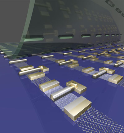 |
| Self-aligned graphene transistor.
|
|
Now, researchers from the California NanoSystems Institute at UCLA, the UCLA Department of Chemistry and Biochemistry, and the department of materials science and engineering at the UCLA Henry Samueli School of Engineering and Applied Science have developed a successful, scalable method for fabricating self-aligned graphene transistors with transferred gate stacks (see paper in PNAS: "High-frequency self-aligned graphene transistors with transferred gate stacks").
|
|
By performing the conventional lithography, deposition and etching steps on a sacrificial substrate before integrating with large-area graphene through a physical transferring process, the new approach addresses and overcomes the challenges of conventional fabrication. With a damage-free transfer process and a self-aligned device structure, this method has enabled self-aligned graphene transistors with the highest cutoff frequency to date — greater than 400 GHz.
|