|
|
|
|
(Nanowerk News) IEMN (Institute of Electronics, Microelectronics and Nanotechnology), one of the largest technological facilities in France, and Digital Surf, provider of software solutions for surface imaging and metrology based on its Mountains Technology®, confirm that they have entered into a technical cooperation agreement.
|
|
IEMN has joined Digital Surf's Mount Shasta technical cooperation programme with internationally reputed laboratories engaged in scientific research. One of the core areas of research at IEMN is the physics of nanostructures and quantum devices. In this area, a major domain of experimental activity is the development of state of the art measurement methods and tools mainly based on scanning probe microscopy to enable the characterization of nanostructures.
|
|
Digital Surf's MountainsMap® surface imaging and metrology software is used with a wide range of micro and nanoscale imaging and measuring systems, including scanning tunneling microscopes (STM's), atomic force microscopes (AFM's) and other scanning probe microscopes (SPM's). Under the terms of the agreement with IEMN, Digital Surf is providing IEMN with its MountainsMap® software and the IEMN Physics Group is giving technical feedback pertinent to the evolution of future generations of the software.
|
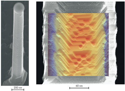 |
| Left: SEM image of a Si nanowire. Right: SEM and STM images – automatically co-localized using MountainsMap® correlative metrology features - show the sawtooth faceted sidewalls of the Si nanowire. While the small Au clusters are barely seen on the SEM image, they are well resolved in STM and are predominantly found on the downward facets of the nanowire sidewall.
|
|
In 2011 the IEMN Physics Group completed the development of a state of the art platform called the Nanoprobe that links our everyday macroscale world and the nanoscale world. Opening up an enormous range of new characterizations in nanotechnology, this platform integrates a multiprobe scanning tunneling microscope with a scanning electron microscope that allows arbitrary arrangements of probe electrodes on a specimen with an unprecedented control on the probe positioning from the tunneling regime to strong electrical contact.
|
|
Operating in an ultra high vacuum environment at variable temperatures (30K - 530K), the platform can carry out a wide range of studies, from fabrication to analysis, without any risk of sample contamination. It combines a preparation chamber that synthesizes nano-objects, a scanning electron microscope and scanning tunneling microscopes that locate them with high precision, and four probe tips that allow 4-point contact measurements and function testing of nanodevices within complex structures and integrated circuits, as well as manipulation of freestanding nanostructures. |
|
There are only a few platforms similar to the Nanoprobe in the world and the Nanoprobe is the only such platform in France. Providing a better insight into the properties of novel semiconductor nanostructures will help to pave the way to their integration into future generations of industrial systems and consumer products including information technology infrastructures, computers, cell phones and other electronic devices. Once this has been achieved these systems and products will have higher performance, consume much less energy and have significantly longer in-service life - with benefits for everyone.
|
|
Within this context, IEMN scientists have already used Digital Surf’s MountainsMap® software in the characterization of nanowire morphology. Understanding the morphology of nanowires, which depends upon their growth conditions, is crucial to determining their physical properties and integrating them into devices. On a silicon nanowire sample studied at IEMN scanning electron microscopy and scanning tunneling microscopy both revealed the existence of sawtooth facets due to small gold clusters. Using MountainsMap® software the SEM and STM images can be correlated and the orientations and atomic structure of the facets can be unambiguously determined.
|
|
"We are very pleased to add MountainsMap® to IEMN's set of state of the art tools," stated Bruno Grandidier, research scientist at the Centre National de la Recherche Scientifique (National Centre for Scientific Research) and leader of the IEMN team that operates the Nanoprobe platform. "The software’s surface visualization and analysis capabilities greatly facilitate the characterization of nanomaterials."
|
|
"The evolution of our software solutions for nano surface characterization will benefit significantly from feedback from IEMN, which has great experience and distinction in nanotechnology research and education," stated François Blateyron, COO of Digital Surf.
|
|
IEMN (Institute of Electronics, Microelectronics and Nanotechnology) was founded in Lille, France in 1992 by associating the CNRS (National Centre for Scientific Research), the University of Lille 1, the University of Valenciennes and Hainaut Cambrésis and ISEN (the Higher Institute for Electronics and Digital Technology). A major European research institute and one of the biggest in France, IEMN is dedicated to electronics in the broadest sense, from the physics of materials and nanostructures to telecommunications systems and acoustic and microwave instrumentation. There is a special focus on micro and nanotechnology, including nanostructures, nanoelectronics, microsystems and microwave. Carrying out research on an international level, IEMN provides higher education on the Masters, Doctoral and Post-doctoral levels, and is committed to the promotion of research and the transfer of knowledge in the interests of society and the economy. http://exploit.iemn.univ-lille1.fr/ http://www.isen.fr/recherche/STM/
|
|
Digital Surf, founded in 1989, specializes in providing surface analysis software for all types of surface metrology instrument including 2D and 3D profilometers, optical interferometric and confocal microscopes, and scanning probe microscopes. Imaging and analysis software based on Digital Surf’s Mountains Technology® is integrated by leading instrument manufacturers and is used in thousands of laboratories and industrial facilities working in numerous sectors including aerospace, automotive, cosmetics, energy, MEMS, materials research, medical, metallurgy, nanostructures, optics, paper, PCB, plastics, polymers, printing, semiconductor, etc.
|