| Sep 06, 2012 |
Researchers demonstrate low-noise, chip-based optical wavelength converter
|
|
(Nanowerk News) Researchers from the NIST Center for Nanoscale Science and Technology have demonstrated a low-noise device for changing the wavelength of light using nanofabricated waveguides created on a silicon-based platform using standard planar fabrication technology ("Low-noise chip-based frequency conversion by four-wave-mixing Bragg scattering in SiNx waveguides").
|
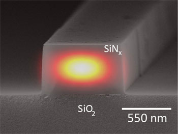 |
| Scanning electron micrograph of the cross-section of a silicon nitride waveguide designed for the low-noise frequency conversion with a simulation of the device's optical field profile superimposed.
|
|
Optical wavelength conversion is an important resource for applications in both classical and quantum information processing: it can connect physical systems operating at different wavelengths, and facilitate improved light detection by converting light to wavelengths for which highly sensitive detectors are available. However, for many such applications the conversion process must not introduce additional noise.
|
|
The researchers were able to demonstrate noise-free wavelength conversion using silicon nitride waveguides fabricated on a silicon substrate. These waveguides were designed based on electromagnetic simulations to determine an appropriate device geometry for a process called four-wave-mixing Bragg scattering, where an input signal field is converted to an output field whose frequency is shifted from the original by an amount equal to the difference in the frequencies of two applied pump fields.
|
|
Measurements show conversion efficiencies in these devices as high as a few percent, approaching the levels needed for some applications, and with no excess noise added during the conversion process. These new noise-free frequency converters are dramatically smaller than the nonlinear crystals and optical fibers used in previous work (by several orders of magnitude), and can be created in arrays and integrated with other on-chip devices using scalable silicon-based fabrication methods.
|
|
Future work will focus on increasing the conversion efficiency levels by optimizing the waveguide geometry and incorporating the waveguides into optical resonators.
|