| Nov 08, 2012 |
Millimeter-wave oscillation by ferromagnetic nanocontact device
|
|
(Nanowerk News) Hiroshi Imamura and Hiroko Arai, Theory Team, the Spintronics Research Center of the National Institute of Advanced Industrial Science and Technology (AIST), have demonstrated theoretically that oscillation of 5–140 GHz is possible by supplying direct current to a ferromagnetic nanocontact device.
|
|
Conventional giant magnetoresistive devices or ferromagnetic tunnel junction devices provide only low frequency oscillation and have been deemed unsuitable for applications requiring millimeter-wave (30–300 GHz) oscillation, including radar. However, upon analyzing precessional motion of spin induced by supplying a current to a ferromagnetic nanocontact device using a simulator developed by AIST, it was predicted that varying the current supplied to the ferromagnetic nanocontact device would cause the device to act as a current control-type oscillation device in the microwave to millimeter-wave range. If such a ferromagnetic nanocontact device is realized, it is expected to have applications in next-generation wireless communication technology and sensor technology.
|
|
Details of the results will be published online shortly in Applied Physics Letters.
|
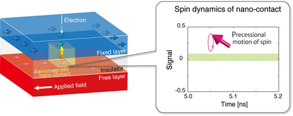 |
| Schematic diagram of ferromagnetic nanocontact device (left) and oscillation behavior in high-frequency range (right).
|
|
Social Background of Research
|
|
The rapid progress in microfabrication technology in recent years has made it possible to make nanometer-scale devices using ferromagnetic materials. Currently, highly functional spintronic devices that actively utilize spin, a characteristic of electrons as magnets, as well as the electricity (electric charges) of electrons, have been developed and put to practical use. Typical examples of spintronic devices include giant magnetoresistive devices and ferromagnetic tunnel junction devices. These devices are used in hard disk reading heads and magnetic resistance random access memories (MRAMs) as non-volatile memory cells, providing a foundation of high-capacity, high-speed data recording technology.
|
|
Aside from applications in the field of data recording technology, oscillating and receiving devices, etc., are being developed that use precessional motion of the spin in magnetic materials oscillating at frequencies corresponding to microwaves. It is predicted that oscillating and receiving devices of the nanometer size would have higher spatial resolution and higher-sensitivity than conventional devices, so these are expected to have applications in high-frequency technology and in wireless communications between minute devices. However, giant magnetoresistive devices or ferromagnetic tunnel junction devices provide only microwave frequency oscillation between 10 GHz and 20 GHz and has been considered unsuitable for applications requiring millimeter-wave oscillating frequencies, including sensors and radar. An additional issue is that the range of frequencies that can be controlled has been too narrow for wireless communication technology.
|
|
History of Research
|
|
AIST has conducted research and development with the aim of the applications of high-performance ferromagnetic tunnel junctions in high-frequency technology. It discovered that high-performance ferromagnetic tunnel junctions work as diodes that demodulate high-frequency signals, and developed a method for precisely evaluating the operation of spintronic devices using this effect (AIST Press Releases on November 17, 2005 and November 26, 2007). AIST has also achieved oscillation output of larger than 0.1 µW, which is more than 100 times larger than that of a giant magnetoresistive device (AIST Press Release on August 28, 2008). Since 2009, AIST has collaborated with a research group led by Professor Masashi Sahashi of Tohoku University to develop ultra-small microwave oscillation devices using ferromagnetic nanocontacts, resulting in the present theoretical proposal for a current control-type oscillation device.
|
|
Part of this research and development was conducted through an innovative energy conservation technology development project/challenge research, "Development of an inter-chip signal transmission microwave oscillation device" (FY2009–FY2011), commissioned by the New Energy and Industrial Technology Development Organization in cooperation with the research group of Professor Sahashi (the person responsible for the project).
|
|
Details of Research
|
|
The ferromagnetic nanocontact used in simulation was a 4-nanometer cube with insulators covering the lateral sides, while the top and bottom were sandwiched between metal electrodes of ferromagnetic material (Fig. 1). The spin of the upper side's ferromagnetic electrode (fixed layer) was fixed in one direction, while that of the lower side's ferromagnetic electrode (free layer) could move freely. When an external magnetic field is applied and the directions of magnetization of the free and fixed layers are made antiparallel, the twisted spin structure called a magnetic wall can be enclosed in the ferromagnetic nanocontact. If electrons are injected from the fixed layer side in this state, a current with uniform spin directions (spin current) flows through the nanocontact, causing the spin in the nanocontact to start rotational motion as a result of spin torque, so that spin waves occur in the free layer that is in contact with the ferromagnetic nanocontact.
|
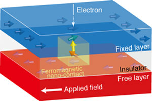 |
| Figure1: Schematic diagram of ferromagnetic nanocontact and ferromagnetic electrodes. The magnetic wall can be enclosed in the ferromagnetic nanocontact.
|
|
The current dependence of the oscillating frequency of the spin wave as found by the simulation can be categorized into three characteristic regions, A, B, and C (Fig. 2). Spatially, the spin wave spreads through the entire free layer in regions A and C but occurs only locally, close to the nanocontact, in region B. It is understood that with oscillations in regions A and C, oscillating frequency is determined by the characteristics of the free layer, but with oscillations in region B, oscillating frequency is determined by the precessional motion of the magnetic wall enclosed in the nanocontact. The spin structure of the magnetic wall in the nanocontact varies according to the value of the spin current flowing through the nanocontact, and therefore it is possible to continuously control the frequency of the oscillation in region B in a range of 5–140 GHz by varying the spin current density.
|
|
If such a device is realized, it is expected to break through the limits of oscillating frequency with giant magnetoresistive devices and ferromagnetic tunnel junction devices and to contribute greatly to the realization of high-speed wireless communications between chips mounted in three dimensions and of nanosized living body sensors using millimeter waves.
|
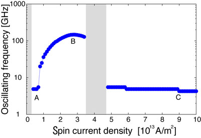 |
| Figure 2: Current density dependence of oscillating frequency. Oscillations can be categorized into three characteristic regions, A, B, and C. The gray area indicates a region with no oscillation.
|
|
Future Plans
|
|
The researchers will prototype and evaluate high-frequency oscillation devices based on this theoretical proposal, do research and development of receiving devices, and conduct research to realize wireless communication systems using ferromagnetic nanocontacts.
|