| Dec 29, 2012 | |
Military projects and nanotechnology push boundaries of flexible electronics in imaging technologies |
|
| (Nanowerk News) Aiming to address the strategic military need for accurate, high-resolution imaging, a University of Wisconsin-Madison electrical and computer engineer working with the U.S. Air Force Office of Scientific Research and the U.S. Department of Defense has a simple goal: to make night vision more accurate and easier for soldiers and pilots to use. | |
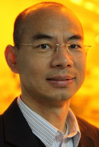 Jack Ma Through some key breakthroughs in flexible semiconductors, electrical and computer engineering Professor Zhenqiang "Jack" Ma has created two imaging technologies that have potential applications beyond the 21st century battlefield. With $750,000 in support from the Air Force Office of Scientific Research (AFOSR), Ma has developed curved night-vision goggles using germanium nanomembranes. Creating night-vision goggles with a curved surface allows a wider field of view for pilots, but requires highly photosensitive materials with mechanical bendability-the silicon used in conventional image sensors doesn't cut it. Instead, Ma's design employs flexible germanium nanomembranes: a transferrable flexible semiconductor that until now has been too challenging to use in imagers due to a high dark current, the background electrical current that flows through photosensitive materials even when they aren't exposed to light. |
|
| "Because of their higher dark current, the image often comes up much noisier on germanium-based imagers," says Ma. "We solved that problem." | |
| Ma's dark current reduction technology has also been recently licensed to Intel. | |
| In another imaging project, the U.S. Department of Defense has provided Ma with $750,000 in support of development of imagers for military surveillance that span multiple spectra, combining infrared and visible light into a single image. | |
| "The reason they are interested in IR is because visible light can be blocked by clouds, dust, smoke," says Ma. "IR can go through, so simultaneous visible and IR imaging allows them to see everything." | |
| Inexpensive silicon makes production of visible light imagers a simple task, but IR relies on materials incompatible with silicon. | |
| The current approach involves a sensor for IR images and a sensor for visible light, combining the two images in post-processing, which requires greater computing power and hardware complexity. Instead, Ma will employ a heterogeneous semiconductor nanomembrane, stacking the two incompatible materials in each pixel of the new imager to layer IR and visible images on top of one another in a single image. | |
| The result will be imagers that can seamlessly shift between IR and visible images, allowing the picture to be richer and more quickly utilized for strategic decisionmaking. | |
| "They are looking for the highest resolution they can get," says Ma. "Something that can take one picture with everything in it." |
| Source: University of Wisconsin-Madison |