| Jan 04, 2013 |
New 2D material for next generation high-speed electronics
|
|
(Nanowerk News) A new two-dimensional material – made up of layers of crystal known as molybdenum oxides – has unique properties that encourage the free flow of electrons at ultra-high speeds.
|
|
In a paper published in the January issue of materials science journal Advanced Materials ("Enhanced Charge Carrier Mobility in Two-Dimensional High Dielectric Molybdenum Oxide"), the researchers explain how they adapted a revolutionary material known as graphene to create a new conductive nano-material.
|
 |
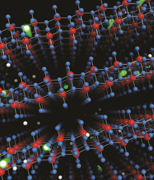
| Artist impression of high carrier mobility through layered molybdenum oxide crystal lattice. (Image: Dr Daniel J White, ScienceFX)
|
|
Graphene was created in 2004 by scientists in the UK and won its inventors a Nobel Prize in 2010. While graphene supports high speed electrons, its physical properties prevent it from being used for high-speed electronics.
|
|
The CSIRO's Dr Serge Zhuiykov said the new nano-material was made up of layered sheets – similar to graphite layers that make up a pencil's core.
|
|
"Within these layers, electrons are able to zip through at high speeds with minimal scattering," Dr Zhuiykov said.
|
|
"The importance of our breakthrough is how quickly and fluently electrons – which conduct electricity – are able to flow through the new material."
|
|
RMIT's Professor Kourosh Kalantar-zadeh said the researchers were able to remove "road blocks" that could obstruct the electrons, an essential step for the development of high-speed electronics.
|
|
"Instead of scattering when they hit road blocks, as they would in conventional materials, they can simply pass through this new material and get through the structure faster," Professor Kalantar-zadeh said.
|
|
"Quite simply, if electrons can pass through a structure quicker, we can build devices that are smaller and transfer data at much higher speeds.
|
|
"While more work needs to be done before we can develop actual gadgets using this new 2D nano-material, this breakthrough lays the foundation for a new electronics revolution and we look forward to exploring its potential."
|
|
In the paper titled 'Enhanced Charge Carrier Mobility in Two-Dimensional High Dielectric Molybdenum Oxide,' the researchers describe how they used a process known as "exfoliation" to create layers of the material ~11 nm thick.
|
|
The material was manipulated to convert it into a semiconductor and nanoscale transistors were then created using molybdenum oxide.
|
|
The result was electron mobility values of >1,100 cm2/Vs – exceeding the current industry standard for low dimensional silicon.
|
|
The work, with RMIT doctoral researcher Sivacarendran Balendhran as the lead author, was supported by the CSIRO Sensors and Sensor Networks Transformational Capability Platform and the CSIRO Materials Science and Engineering Division.
|
|
It was also a result of collaboration between researchers from Monash University, University of California – Los Angeles (UCLA), CSIRO, Massachusetts Institute of Technology (MIT) and RMIT.
|

