| Jan 30, 2013 | |
Downsizing photonic devices to the scale of computer chips (w/video) |
|
| (Nanowerk News) Optical communications, or photonics, technology has failed to match the miniaturization of electronic components, mainly because of fundamental laws of classical optics. The smallest photonic devices are limited to sizes of at least a micrometer. | |
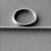 Microscopy image of a waveguide-ring resonator; ring diameter is approximately 5 micrometers. Researchers from the A*STAR Institute of Microelectronics (IME) in Singapore have now realized a device design that beats such size restrictions and can be easily integrated into a silicon chip ("Performance of ultracompact copper-capped silicon hybrid plasmonic waveguide-ring resonators at telecom wavelengths"). Using so-called ‘plasmonic techniques’, the researchers, led by Shiyang Zhu at the IME, demonstrated optical resonator structures, which allow a beam of light to circulate in a closed path, that can be used as on-off switches for light. The device is based on plasmonic effects that guide the light along the surface of the metal. “The performance of our devices is comparable to the best reported results for related plasmonic resonators,” says Zhu. Conventional optical instruments, such as lenses, modify light as it passes through them. Plasmonic structures, however, act more like antennae that amplify light as it moves along their surface. Plasmonic features are typically created using metals such as gold or silver. However, integrating these noble metals with silicon chips is not only expensive, but also requires techniques that are incompatible with established silicon processing techniques. |
|
| As a workaround, Zhu and co-workers used copper to generate the desired plasmonic effects. Copper is widely used as electronic wires in silicon computer chips, and it has an established track record in the computer industry. The researchers built their plasmonic resonator devices from two copper structures that guide light along them — a long wire adjacent to a circle (see image). The smallest width of the copper circuit is only about 180 nanometers, which is much smaller than conventional light guides. | |
| The closeness of the wire and the circle is critical for efficient device operation. When light of a specific wavelength, which is determined by the dimensions of the circle, passes through the wire, some of it can leak into the circle (see video) where it becomes trapped. Light can only pass through the structure if it does not match the resonance wavelength of the circle. | |
| The wavelength at which this resonance occurs is very sensitive to parameters such as temperature. In the future, this sensitivity in the circuits could be harnessed for use as switches that control how light passes through the wire, says Zhu. “The next step is to design and demonstrate active plasmonic devices, such as thermo-optic switchers and high-speed electro-optic modulators.” |
| Source: A*STAR |