| Feb 13, 2013 |
New model makes designing nanoelectronic materials significantly simpler
|
|
(Nanowerk News) Advances in miniaturization have made electronic devices cheaper and more powerful, but these procedures also create new challenges for materials scientists. For example, traditional silicon dioxide insulators used in field-effect transistors begin to leak small amounts of current at nanoscale dimensions. To combat this problem, researchers have developed insulators called ‘high-k dielectrics’ that link heavier elements, such as hafnium or zirconium, into insulating oxide films with exceptional charge-isolating capabilities.
|
|
Integrating high-k dielectrics into circuits, however, creates a different manufacturing problem. Localized electric fields known as charged dipoles can form at insulator–semiconductor interfaces and generate unwanted voltages that impact device performance. Sing Yang Chiam from the A*STAR Institute of Materials Research and Engineering in Singapore and co-workers have now developed a model that can identify interface dipole problems before they appear ("An interface dipole predictive model for high-k dielectric/semiconductor heterostructures using the concept of the dipole neutrality point ") — a finding that promises to help end the ‘trial-and-error’ design issues typical of high-k dielectrics.
|
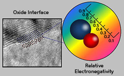 |
| A new theoretical model enables accurate predictions of dipoles at oxide interfaces (left, electron microscopy image) using the classical property of electronegativity (right). The scale shows how two elements with different relative electronegativities align at an interface.
|
|
Currently, materials scientists employ extensive quantum mechanical calculations to determine whether or not new high-k dielectrics will have interface dipoles. Chiam and co-workers investigated a more intuitive approach: they linked the appearance of interface dipoles to the classical property of electronegativity, a number that relates an element’s electron-attracting power to its position in the periodic table.
|
|
Scientists have previously avoided estimating dipoles with electronegativity values because, in many cases, they predict incorrect electric field polarities. To resolve this discrepancy, Chiam and co-workers correlated theoretical electronegativity with experimental ‘charge neutrality levels’ — electronic energies required to counterbalance dipoles on insulator interfaces. After measuring the charge neutrality on several different high-k dielectrics with X-ray and ultraviolet radiation (see image), the team plotted this data against electronegativity. They discovered that a simple linear equation connected the two parameters.
|
|
Further manipulation of this equation revealed it could also predict a so-called ‘dipole neutrality point’ (DNP) where interfacial dipoles flip polarity. Armed with this new theoretical tool, the researchers investigated both well-known and novel high-k dielectric/semiconductor interfaces. They found that the DNP concept provided accurate predictions of dipole polarity and strength: the offset voltages needed to turn on a high-k dielectric field-effect transistor closely matched values generated from the electronegativity values.
|
|
Chiam notes that the straightforwardness of this model should make it exceptionally practical for scientific discovery. “This is the simplest method to find dipoles at material interfaces before starting experiments,” he says. “Our model can predict what kinds of bulk or interface modifications are needed to offset dipole values — a significant time saving over traditional approaches.”
|