| Mar 13, 2013 |
Surprising control over photoelectrons from a topological insulator
|
|
(Nanowerk News) Plain-looking but inherently strange crystalline materials called 3D topological insulators (TIs) are all the rage in materials science. Even at room temperature, a single chunk of TI is a good insulator in the bulk, yet behaves like a metal on its surface.
|
|
Researchers find TIs exciting partly because the electrons that flow swiftly across their surfaces are “spin polarized”: the electron’s spin is locked to its momentum, perpendicular to the direction of travel. These interesting electronic states promise many uses – some exotic, like observing never-before-seen fundamental particles, but many practical, including building more versatile and efficient high-tech gadgets, or, further into the future, platforms for quantum computing.
|
|
A team of researchers from the U.S. Department of Energy’s Lawrence Berkeley National Laboratory (Berkeley Lab) and the University of California at Berkeley has just widened the vista of possibilities with an unexpected discovery about TIs: when hit with a laser beam, the spin polarization of the electrons they emit (in a process called photoemission) can be completely controlled in three dimensions, simply by tuning the polarization of the incident light.
|
|
“The first time I saw this it was a shock; it was such a large effect and was counter to what most researchers had assumed about photoemission from topological insulators, or any other material,” says Chris Jozwiak of Berkeley Lab’s Advanced Light Source (ALS), who worked on the experiment. “Being able to control the interaction of polarized light and photoelectron spin opens a playground of possibilities.”
|
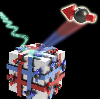 |
| The interior bulk of a topological insulator is indeed an insulator, but electrons (spheres) move swiftly on the surface as if through a metal. They are spin-polarized, however, with their momenta (directional ribbons) and spins (arrows) locked together. Berkeley Lab researchers have discovered that the spin polarization of photoelectrons (arrowed sphere at upper right) emitted when the material is struck with high-energy photons (blue-green waves from left) is completely determined by the polarization of this incident light. (Image Chris Jozwiak)
|
|
The Berkeley Lab-UC Berkeley team was led by Alessandra Lanzara of Berkeley Lab’s Materials Sciences Division (MSD) and UC Berkeley’s Department of Physics, working in collaboration with Jozwiak and Zahid Hussain of the ALS; Robert Birgeneau, Dung-Hai Lee, and Steve Louie of MSD and UC Berkeley; and Cheol-Hwan Park of UC Berkeley and Seoul National University. They and their colleagues report their findings in Nature Physics ("Photoelectron spin-flipping and texture manipulation in a topological insulator").
|
|
Strange electronic states and how to measure them
|
|
In diagrams of what physicists call momentum space, a TI’s electronic states look eerily like the same kinds of diagrams for graphene, the single sheet of carbon atoms that, before topological insulators came along, was the hottest topic in the materials science world.
|
|
In energy-momentum diagrams of graphene and TIs, the conduction bands (where energetic electrons move freely) and valence bands (where lower-energy electrons are confined to atoms) don’t overlap as they do in metals, nor is there an energy gap between the bands, as in insulators and semiconductors. Instead the “bands” appear as cones that meet at a point, called the Dirac point, across which energy varies continuously.
|
|
The experimental technique that directly maps these states is ARPES, angle-resolved photoemission spectroscopy. When energetic photons from a synchrotron light source or laser strike a material, it emits electrons whose own energy and momentum are determined by the material’s distribution of electronic states. Steered by the spectrometer onto a detector, these photoelectrons provide a picture of the momentum-space diagram of the material’s electronic structure.
|
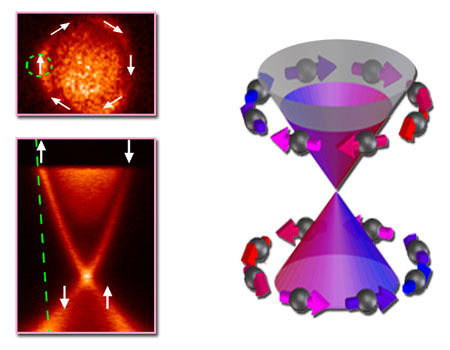 |
| The diagram at right shows the electronic states of bismuth selenide in momentum space. ARPES, at left, can directly create such maps with photoelectrons. A slice through the conduction cone at the Fermi energy maps the topological insulator’s surface as a circle (upper left); here electron spins and momenta are locked together. Initial ARPES measurements in this experiment were made with p-polarized incident light in the regions indicated by the green circle and line, where the spin polarization of the photoelectrons consistent with the intrinsic spin polarization of the surface.
|
|
Similar as their Dirac-cone diagrams may appear, the electronic states on the surface of TIs and in graphene are fundamentally different: those in graphene are not spin polarized, while those of TIs are completely spin polarized, and in a peculiar way.
|
|
A slice through the Dirac-cone diagram produces a circular contour. In TIs, spin orientation changes continuously around the circle, from up to down and back again, and the locked-in spin of surface electrons is determined by where they lie on the circle. Scientists call this relation of momentum and spin the “helical spin texture” of a TI’s surface electrons. (Electron spin isn’t like that of a spinning top, however; it’s a quantum number representing an intrinsic amount of angular momentum.)
|
|
Directly measuring the electrons’ spin as well as their energy and momentum requires an addition to ARPES instrumentation. Spin polarization is hard to detect and in the past has been established by firing high-energy electrons at gold foil and counting which way a few of them bounce; collecting the data takes a long time.
|
|
Jozwiak, Lanzara, and Hussain jointly led the development of a precision detector that could measure the spin of low-energy photoelectrons by measuring how they scatter from a magnetic surface. Called a spin time-of-flight analyzer, the device is many times more efficient at data collection.
|
|
Says Hussain, “It’s the kind of project that could only be done at a place like Berkeley Lab, where tight collaboration for a wide range of capabilities is possible.”
|
|
The new instrument was first used at the ALS to study the well-known topological insulator bismuth selenide. While the results confirmed that bismuth selenide’s helical spin texture persists even at room temperature, they raised a perplexing question.
|
|
Lanzara says, “In an ARPES experiment, it’s usually assumed that the spin polarization of detected photoelectrons accurately reports the spin polarization of electrons within the material.” She explains that “this assumption is frequently made when confirming the helical spin texture of a TI’s surface electrons. But in our spin-ARPES experiments, we found significant deviations between the spin polarizations of the surface electrons versus the photoelectrons. We knew we had to look further.”
|
|
Flipping photoelectron spins
|
|
Probing the TI surface electrons didn’t require the high photon energy of a synchrotron beam, so the new study was primarily done in a laboratory with a laser that could produce intense ultraviolet light capable of stimulating photoemission, and whose polarization was readily manipulated. The experiment used high-quality samples of bismuth selenide from Birgeneau’s MSD and UC Berkeley labs.
|
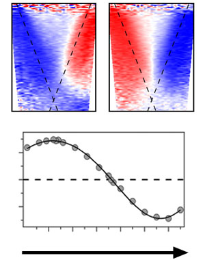 |
| Incident light that’s p-polarized (upper left) produces photoelectrons consistent with the usual picture of spin polarization in a topological insulator’s surface, but changing the polarization of the incident light also changes the spin polarization of the photoelectrons.
|
|
In the first experiments, the incident light was p-polarized, which means the electric part of the light wave was parallel to a plane that was perpendicular to the TI surface and oriented according to the path of the emitted photoelectrons. Since studies of topological insulators typically use p-polarized light in this geometry, sure enough, the spin-ARPES measurements showed the photoelectrons were indeed spin polarized in directions consistent with the expected spin texture of the surface electrons.
|
|
“After we’d measured p-polarization, we switched to an s-polarized laser beam,” Jozwiak says. “It only took a few minutes to collect the data.” (S-polarization means the electric part of the light wave is perpendicular to the same imaginary plane – perpendicular in German being senkrecht.)
|
|
Three minutes after he started the run, Jozwiak got a jolt. “The experiment was completely the same, except for the light polarization, but now the photoelectrons were spin polarized in the reverse direction – the opposite of what you’d expect.” His first assumption was “I must have done something wrong.”
|
|
Repeated careful experiments with a range of laser polarizations showed, however, that the spin polarization of the photons in the laser beam controlled the polarization of the emitted photoelectrons. When the laser polarization was smoothly varied – and even when it was circularly polarized right or left – the photoelectron spin polarization followed suit.
|
|
Why had no results counter to the expected surface textures been reported before? Probably because the most common kind of spin-ARPES experiment makes a few measurements in a typical geometry using p-polarized light. With other arrangements, however, photoelectron spin polarization departs markedly from expectations.
|
|
The team’s theory collaborators, Park, Louie, and Lee, helped explain the unusual theoretical results when they predicted that just such differences between photoelectron and intrinsic textures should occur. There are also suggestions that the simple picture of spin texture in topological insulators is more complex than has been assumed. Says Lanzara, “It’s a great motivation to keep digging.”
|
|
The ability to hit a topological insulator with a tuned laser and excite polarization-tailored electrons has great potential for the field of spintronics – electronics that exploit spin as well as charge. Devices that optically control electron distribution and flow would constitute a significant advance.
|
|
Optical control of TI photoemission has more immediate practical possibilities as well. Bismuth selenide could provide just the right kind of photocathode source for experimental techniques that require electron beams whose spin polarization can be exquisitely and conveniently controlled.
|