| Mar 26, 2013 |
FinFET with the world's smallest characteristics variability
|
|
(Nanowerk News) Takashi Matsukawa and Meishoku Masahara and others, Silicon Nano-Device Group, the Nanoelectronics Research Institute of the National Institute of Advanced Industrial Science and Technology (AIST), have developed a prototype of a 14 nm-generation 3D transistor (FinFET) with the world’s smallest variability of characteristics (Fig. 1 left)
|
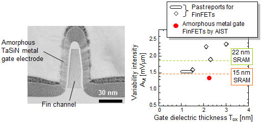 |
| Figure 1: Low-variability FinFET prototype (left) and a comparison with past reports on characteristics variability intensity (right).
|
|
A primary cause of the characteristics variability in a FinFET is the variability of physical properties of the metal gate electrode material. An amorphous metal material for the gate electrode that has a small variability of physical properties has been developed and the prototype FinFET with the world’s smallest characteristics variability was fabricated using the material. With integrated circuits beyond the 14 nm generation, including SRAMs (static random access memories), major issues have been the hindrance to performance improvement and the reduction in yields, both due to the characteristics variability of elements. The present results are expected to contribute to solving these issues.
|
|
Details of this technology have been presented at the 2012 International Electron Devices Meeting (IEDM 2012) held in San Francisco, U.S.A., from December 10 to 12, 2012.
|
|
Social Background of Research
|
|
Until now, the performance improvement and the integration scale increase of silicon integrated circuits have been achieved by miniaturizing the transistors, which are the smallest elements of these circuits. The miniaturization of transistors is also linked to cost reduction, and thus fierce competition to develop more miniaturized transistors continues. However, in the technology used for the 14 nm-generation transistor, which is expected to be in production after 2017, there will be issues with variability of characteristics among transistor elements due to their small size. There is concern about the hindrance to the performance improvement of products and the reduction in yields. In particular, SRAMs, which occupy more than 50 % of the area of system LSIs (large-scale integrated circuits) and microprocessors, can be easily affected by the variability of characteristics owing to the intensive use of smallest transistors in their circuits. For these reasons, there is strong need to develop miniaturized transistors with small characteristics variability.
|
|
History of Research
|
|
AIST has been conducting research in transistors with new structure called FinFETs that have a three-dimensional structure. In addition, AIST proposed a four-terminal FinFET to electrically control the parameter of the transistor, and it demonstrated the operation of this transistor in 2003. Furthermore, AIST proposed that the variability of physical properties of the metal gate electrode material was a new factor affecting the characteristics variability of FinFETs in 2008. This was followed by the proposal of a new transistor-manufacturing technology that enabled the reduction of the variability of physical properties. AIST also identified the primary factor causing the variability of on-state current in 14 nm-generation FinFETs (AIST press release on December 8, 2011). AIST has since been continuing its research and development efforts to suppress the variability of characteristics in FinFETs.
|
|
This research was conducted as part of the project “Technology Development of New Nanoelectronics Semiconductor Materials and New-Structure Nanoelectronic Devices” (FY2009 - 2011) commissioned by the New Energy and Industrial Technology Development Organization.
|
|
Details of Research
|
|
Characteristics variability, which has become significant in miniaturized transistors, is mainly classified into two types, manifesting itself as off-state current variability and on-state current variabitity and having adverse effects on the performance of integrated circuits. The variability of off-state current exponentially increases the off-state current of some of transistors in an integrated-circuit chip relative to the design value, thus dramatically increasing the standby power consumption of the entire chip. Further, because the operational speed of an integrated circuit is limited by the transistor having the lowest on-state current in the integrated circuit, the variability of on-state current reduces the operational speed of the circuit to lower than the design value. In other words, the advancement in the miniaturization of transistors has been accompanied by serious problems, such as operational speed has not increased while power consumption has.
|
|
In FinFETs introduced with the 22 nm generation, the primary cause of characteristics variability is the variability of a physical property, called the work function, of the gate electrodes. The threshold voltage, one of the critical electrical properties of transistors, is determined by the work function of the metal gate electrode material. The material generally used in the metal gate electrodes has a polycrystalline structure, in which the interfaces of individual crystal grains (grain boundaries) have a variety of work functions, resulting in threshold voltage variability (Fig. 2).
|
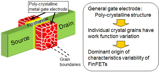 |
| Figure 2: Primary factor causing the threshold voltage variability in a FinFET.
|
|
Therefore, instead of conventional polycrystalline metals (such as titanium nitride, TiN), the researchers used an amorphous metal (tantalum silicon nitride, TaSiN), which has no grain boundary, for the gate electrodes. They then compared variabilities of electrical characteristics. Figure 3 shows electron microscope images of the fin cross-section with the amorphous TaSiN metal gate electrodes developed in this project, compared with that of the conventional polycrystalline TiN metal gate electrodes. The amorphous TaSiN metal gate electrodes were uniformly formed on the side walls of the fin channel, and the grain boundaries that cause the variability in the TiN electrodes is not found. Further, with the TiN electrodes, electron beam diffraction of a periodic and discrete spot pattern can be observed, reflecting the crystal structure. However, with the TaSiN electrodes, only a ring-shaped electron beam diffraction pattern can be observed, suggesting the lack of periodicity and indicating that the amorphous TaSiN metal gate electrodes are appropriately formed on the fin channel.
|
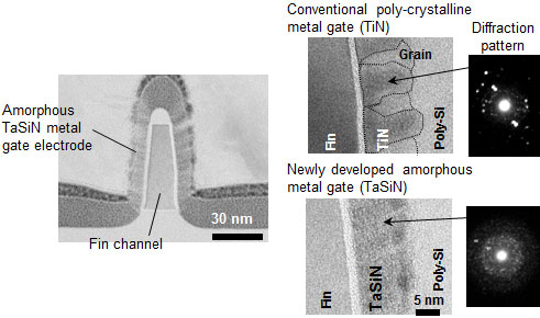 |
| Figure 3: Comparison between the developed FinFET with amorphous TaSiN metal gates and the conventional FinFET with polycrystalline TiN metal gates.
|
|
Among the electrical characteristics variabilities of developed FinFET prototypes with a variety of design dimensions, threshold voltage variability and transconductance variability were analyzed. Figure 4 is a Pelgrom plot of the measured threshold voltage variability. Smaller slope of the plot indicates smaller characteristics variability. Through the use of amorphous TaSiN metal gates, the threshold voltage variability was considerably reduced compared with polycrystalline metal gates. It showed the best minimum value (1.34 mVµm) ever reported for FinFETs (Fig. 1 right). This value fulfills the requirement for proper operation of a 15 nm-generation SRAM. In other words, this technology contributes to a breakthrough in the solution of the threshold voltage variability issue accompanying the miniaturization of transistors.
|
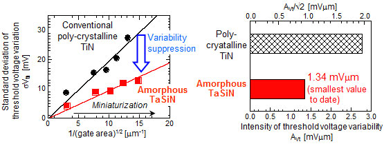 |
| Figure 4: Pelgrom plots comparing the threshold voltage variabilities of the amorphous TaSiN metal gates and the conventional polycrystalline TiN metal gates.
|
|
Figure 5 shows a comparison of transconductance variabilities for gate lengths of 100 nm and 50 nm. As with the threshold voltage variability, the transconductance variability also increases as the gate length decreases; however, through the use of amorphous metal gate electrodes, the variability increase can be drastically reduced. Since transconductance variability is a primary cause for the variability of on-state current in 14 nm-generation (and beyond) transistors, these FinFETs using amorphous metal gate electrodes are expected to help solve the on-state current variability issue in the 14 nm-generation (and beyond) transistors. In addition, they are expected to contribute to solving the low yield problem of integrated circuits such as SRAMs and to achieving low power consumption while enhancing the performance of integrated circuits. This technology is available not only to device manufacturers but also to manufacturers of semiconductor-fabrication systems, materials, and measuring and test devices. The researchers are conducting this research having technology transfer to and collaboration with these corporations in mind.
|
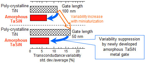 |
| Figure 5: Suppression effects on transconductance variability by the developed amorphous TaSiN metal gates.
|
|
Future Plans
|
|
In the future, the researchers will fabricate integrated circuits using FinFETs aiming at the circuit level validation of their reduced power consumption and improved yields.
|