| Apr 03, 2013 |
Building quantum states with individual silicon atoms
|
|
(Nanowerk News) By introducing individual silicon atom ‘defects’ using a scanning tunnelling microscope, scientists at the London Centre for Nanotechnology have coupled single atoms to form quantum states.
|
|
Published today in Nature Communications ("Quantum engineering at the silicon surface using dangling bonds"), the study demonstrates the viability of engineering atomic-scale quantum states on the surface of silicon – an important step toward the fabrication of devices at the single-atom limit.
|
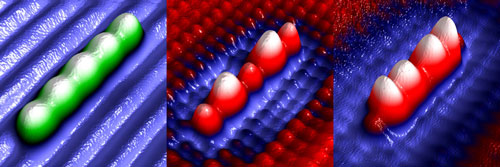 |
| Scanning tunnelling microscopy (STM) images of the quantum states of an artificial atomic defect structure in silicon. This structure was fabricated by using the STM to individually remove five hydrogen atoms from a hydrogen-terminated silicon (001) surface. The absence of the hydrogen atoms creates “dangling bond” states that interact to form extended, artificial molecular orbitals. Only the imaging bias voltage has been changed in the three images shown (from left to right, -1.4, +1.4, and +1.8 Volts).
|
|
Advances in atomic physics now allow single ions to be brought together to form quantum coherent states. However, to build coupled atomic systems in large numbers, as required for applications such as quantum computing, it is highly desirable to develop the ability to construct coupled atomic systems in the solid state.
|
|
Semiconductors, such as silicon, routinely display atomic defects that have clear analogies with trapped ions. However, introducing such defects deterministically to observe the coupling between extended systems of individual defects has so far remained elusive.
|
|
Now, LCN scientists have shown that quantum states can be engineered on silicon by creating interacting single-atom defects. Each individual defect consisted of a silicon atom with a broken, or “dangling”, bond. During this study, these single-atom defects were created in pairs and extended chains, with each defect separated by just under one nanometer.
|
|
Importantly, when coupled together, these individual atomic defects produce extended quantum states resembling artificial molecular orbitals. Just as for a molecule, each structure exhibited multiple quantum states with distinct energy levels.
|
|
The visibility of these states to the scanning tunneling microscope could be tuned through the variation of two independent parameters – the voltage applied to the imaging probe and its height above the surface.
|
|
The study was led by Dr Steven Schofield, who said: “We have created precise arrays of atomic defects on a silicon surface and demonstrated that they couple to form unique and interesting quantum states.”
|
|
He added: “The next step is to replicate these results in other material systems, for example using substitutional phosphorus atoms in silicon, which holds particular interest for quantum computer fabrication.”
|
|
Ongoing research at the LCN is exploring even more complex arrangements of these defects, including the incorporation of impurity atoms within the defect structures, which is expected to alter the symmetry of the defects (similar to the role of the nitrogen atom in the nitrogen-vacancy center defect in diamond).
|