| May 22, 2013 | |
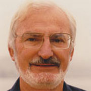
Heinrich Rohrer, co-inventor of the scanning tunneling microscope, has died |
|
| (Nanowerk News) The co-inventor of the scanning tunneling microscope, Dr. Heinrich Rohrer, passed away on the evening of May 16, 2013. He was 79. | |
| Heinrich Rohrer, IBM Fellow and Nobel Laureate, joined the IBM Research Laboratory in Zurich, Switzerland, in December of 1963, where he worked for 34 years. | |
 After hiring a young scientist named Gerd Binnig in the late 1970s, the two started collaborating, brought closely together by their backgrounds in superconductivity and their fascination with atomic surfaces. The two scientists grew increasingly frustrated by the limits of the tools then available to study the distinct characteristics of atomic surfaces, so they decided to build their own, something that would be capable of seeing and manipulating atoms at the nanoscale level. To do that, they began experimenting with tunneling, a quantum phenomenon in which atoms escape the surface of a solid to form a kind of cloud that hovers above the surface; when another surface approaches, the atomic clouds overlap and an atomic exchange occurs. By maneuvering a sharp metal conducting tip over the surface of a sample at extremely close proximity, Binnig and Rohrer found that the amount of electrical current flowing between the tip and the surface could be measured. Variations in this current provided information about the inner structure and the height-relief of the surface. And from this information, one could build a three-dimensional atomic-scale map of the sample’s surface. Gerd Binnig and Heinrich RohrerIn January 1979, Binnig and Rohrer submitted their first patent disclosure on the scanning tunneling microscope (STM). Soon afterwards, with the help of fellow IBM researcher Christoph Gerber, they began to design and construct the microscope itself. |
|
| During their first few months of working on the STM, Binnig and Rohrer had to make a series of adjustments to their original design to produce accurate measurements on such a miniscule scale. These changes led to reductions in vibrations and noise, more precise control of the scanning tip’s location and movement, and improved sharpness of the probe tip itself. | |
| Their first experiment involved the surface structure of a crystal of gold. The resulting images showed rows of precisely spaced atoms and broad terraces separated by steps one atom in height. | |
| More refinements to the microscope improved the precision of the mechanical design and resulted in increasingly clearer images. Soon the significance of Binnig and Rohrer’s invention started reaching scientists around the world, who suddenly had access to the nanoscale world of individual atoms and molecules. | |
| As the STM could also be used to push and pull individual atoms around, it also marked the first time that humans were able to manipulate objects that small. Today, the invention of the STM is considered to have opened the door to nanotechnology. | |
| In awarding Binnig and Rohrer the Nobel Prize in Physics in 1986, just five years after the first STM had been built, the Nobel committee said the invention opened up “entirely new fields... for the study of the structure of matter.” | |
| In 2011, in the presence of 600 guests from throughout the research community, IBM and ETH Zurich dedicated the Binnig and Rohrer Nanotechnology Center in Rüschlikon in honor of the scientists' achievements. | |
| Heinrich Rohrer was as famous for his kindly personality as for his sharp wit and humor. During the opening ceremony of the Nanotechnology Center he participated in a public discussion with Binnig and Dr. Ralph Eicher, president of ETH Zurich. After Binnig attempted to explain their invention, Rohrer jokingly apologized to the audience saying, "If you didn't quite understand what Gerd just told you, you are not alone." |
| Source: IBM |
