| Jul 25, 2013 |
Sub-10 nm nanotechnology engineering breakthrough is big deal for electronics
|
|
(Nanowerk News) University of Akron researchers have developed new materials that function on a nanoscale, which could lead to the creation of lighter laptops, slimmer televisions and crisper smartphone visual displays ("Giant surfactants provide a versatile platform for sub-10-nm nanostructure engineering").
|
|
Known as "giant surfactants" – or surface films and liquid solutions – the researchers, led by Stephen Z.D. Cheng, dean of UA's College of Polymer Science and Polymer Engineering, used a technique known as nanopatterning to combine functioning molecular nanoparticles with polymers to build these novel materials.
|
|
The giant surfactants developed at UA are large, similar to macromolecules, yet they function like molecular surfactants on a nanoscale, Cheng says. The outcome? Nanostructures that guide the size of electronic products.
|
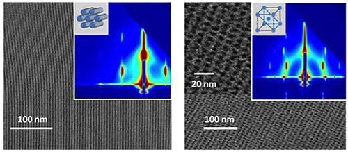 |
| Patterns of two giant surfactant samples in thin-film state.
|
|
More efficient designs possible
|
|
Nanopatterning, or self-assembling molecular materials, is the genius behind the small, light and fast world of modern-day gadgetry, and now it has advanced one giant step thanks to the UA researchers who say these new materials, when integrated into electronics, will enable the development of ultra-lightweight, compact and efficient devices because of their unique structures.
|
|
During their self-assembly, molecules form an organized lithographic pattern on semiconductor crystals, for use as integrated circuits. Cheng explains that these self-assembling materials differ from common block copolymers (a portion of a macromolecule, comprising manyunits, that has at least one feature which is not present in the adjacent portions) because they organize themselves in a controllable manner at the molecular level.
|
|
"The IT industry wants microchips that are as small as possible so that they can manufacture smaller and faster devices," says Cheng, who also serves as the R.C. Musson and Trustees Professor of Polymer Science at UA.
|
|
He points out that the current technique can produce the spacing of 22 nanometers only, and cannot go down to the 10 nanometers or less necessary to create tiny, yet mighty, devices. The giant surfactants, however, can dictate smaller-scale electronic components.
|
|
"This is exactly what we are pursuing — self-assembling materials that organize at smaller sizes, say, less than 20 or even 10 nanometers," says Cheng, equating 20 nanometers to 1 /4,000th the diameter of a human hair.
|
|
Team's work has commercial applications
|
|
An international team of experts, including George Newkome, UA vice president for research, dean of the Graduate School, and professor of polymer science at UA; Er-Qiang Chen of Peking University in China; Rong-Ming Ho of National Tsinghua University in Taiwan; An-Chang Shi of McMaster University in Canada; and several doctoral and postdoctoral researchers from Cheng's group, have shown how well-ordered nanostructures in various states, such as in thin films and in solution, offer extensive applications in nanotechnology.
|
|
"These results are not only of pure scientific interest to the narrow group of scientists, but also important to a broad range of industry people,” says Cheng, noting that his team is testing real-world applications in nanopatterning technologies and hope to see commercialization in the future.
|