| Posted: Jan 22, 2007 | |
Nanowire growth through ion beams |
|
| (Nanowerk Spotlight) Nanowires are expected to play an important role in the emerging fields of nanoelectronics and nanooptics. In particular, the permanently growing complexity of integrated circuit designs requires a further reduction of the size of IC components that nanowires could facilitate. Nanowires are also a possible candidate for future functional nanostructures in plasmonic devices, i.e. for information (light) propagation and manipulation below the optical diffraction limit. For these purposes, cobalt disilicide (CoSi2) is a very promising contact material due to its extremely useful properties such as low resistance, its metallic behavior, its low lattice mismatch to Si of only -1.2%. the plasmon wavelength of 1.2 µm, and its compatibility with modern silicon technology. Many efforts have been made to fabricate silicide nanowires employing the bottom-up approach without elaborate microlithography. Researchers in Germany now have demonstrated a promising technique that allows the defect-induced formation and placing of cobalt disilicide nanowires by focused ion beam synthesis in silicon directly where it is needed. | |
| Focused ion beam (FIB) systems have been produced commercially for approximately ten years, primarily for large semiconductor manufacturers. FIB systems operate in a similar fashion to a scanning electron microscope except, rather than a beam of electrons and as the name implies, FIB systems use a finely focused beam of metal ions (mostly gallium) that can be operated at low beam currents for imaging or high beam currents for site specific sputtering or milling. | |
| In contrast to the usually applied gallium liquid metal ion sources (LMIS), alloy based LMIS provide different ion species and open a broad field of new FIB applications. The researchers in Germany used a combination of a high resolution FIB (top–down approach) and self organization processes during ion beam synthesis (bottom–up approach) to fabricate CoSi2 nanowires in silicon. The obtained nanowires are 10-20 nm in diameter and several micrometers long. | |
| "FIB technology provides a tool that allows us to work on the surface of a material up to 50 nm in depth and to deposit atoms at that depth from which the nanowires are later formed" Dr. Lothar Bischoff explains to Nanowerk. "We are now able to precisely control position and length of nanowires with a diameter between 100 nm to 200 nm." | |
| He points out that they still need to work on achieving better control over the growth of thinner nanowires. "By reducing the FIB dose, the self organisation process becomes more and more dominant, i.e. the nanowire growth starts in the trace but then follows the <110> direction of the silicon lattice due to energetic reasons." | |
| Bischoff is a researcher at the Institute of Ion Beam Physics and Materials Research at the Research Center Dresden-Rossendorf/Germany where they have been working with cobalt disilicide nanowires for several years now. | |
 |
|
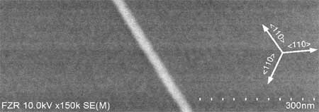
| CoSi2 nanowires in (111)-Si after 30 keV Ga+ FIB implantation and annealing at 1000°C for 30 min. (Reprinted with permission from American Institute of Physics) | |
| "Our main field is the application of high resolution mass separated focused ion beams with a broad spectrum of projectile ions to the fabrication of nanostructures and nanowires" says Bischoff. "Therefore we use techniques such as ion milling, MO-CVD, templating, implantation and ion beam synthesis and defect creation. The combination of bottom-up as well as top-down-approaches, as demonstrated in our recent work, is a promising technique for a further reduction of the feature size of 1D nanostructures." | |
| In a two step fabrication process the Rossendorf researchers first coated SiO2 samples with a 10 nm cobalt film on the rear side (this cobalt layer serves as a reservoir of cobalt atoms during annealing). In a second step, defects are introduced on the front of the sample through FIB implantation of cobalt as well as other ions. Already after 10 minutes of annealing at 1000°C short (200–500 nm) and 10–30 nm thin nanowires self-aligned along the (110) directions were observed independent on the kind of implanted ions. After 30 minutes annealing the wires reach several micrometers in length and 20–50 nm in diameter. | |
| The stability and decay of the nanowires depend on misalignment of the FIB trace with respect to the Si crystal orientation and also on the thermal treatment regime. A small misalignment of the FIB trace of a few degrees leads to the decay of the CoSi2 nanowires into shorter parts and a larger deviation causes a chain of CoSi2 nanoparticles. | |
| Bischoff points out that an advantage of their FIB technique is the ability to implant nanowires from various ion species, e.g. gold or platinum, in different material surfaces. | |
| In a next step, Bischoff and his colleagues will try to combine their CoSi2 nanowires into more complex nanostructures. | |
| These findings have been reported in Applied Physics Letters "Defect induced formation of CoSi2 nanowires by focused ion beam synthesis". | |
| Two previous papers by the researchers report on this technique: "CoSi2 nanostructures by writing FIB ion beam synthesis" in Materials Science & Engineering C and "Investigation of FIB assisted CoSi2 nanowire growth" in Microelectronic Engineering. | |
 By
Michael
Berger
– Michael is author of three books by the Royal Society of Chemistry:
Nano-Society: Pushing the Boundaries of Technology,
Nanotechnology: The Future is Tiny, and
Nanoengineering: The Skills and Tools Making Technology Invisible
Copyright ©
Nanowerk LLC
By
Michael
Berger
– Michael is author of three books by the Royal Society of Chemistry:
Nano-Society: Pushing the Boundaries of Technology,
Nanotechnology: The Future is Tiny, and
Nanoengineering: The Skills and Tools Making Technology Invisible
Copyright ©
Nanowerk LLC
|
Become a Spotlight guest author! Join our large and growing group of guest contributors. Have you just published a scientific paper or have other exciting developments to share with the nanotechnology community? Here is how to publish on nanowerk.com.