| Posted: Jul 09, 2015 | |
Nanoelectronics on textile, paper, wood and stone |
|
| (Nanowerk Spotlight) Nanofabrication techniques often depend on creating a structure on one substrate and then transferring it via various processes onto another, desired, substrate. Nanoimprinting lithography (NIL) is such a pattern transfer process, as is poly(methyl methacrylate) (PMMA)-mediated peeling (see for instance "Free-standing nanosieve membranes that are only 1 nanometer thick"), or transfer printing with a polydimethylsiloxane (PDMS) stamp (for an example of this technique see here: "Nanofabrication enables mass production of non-reflective polymer surfaces" or here: "Printing graphene folds"). | |
| In the field of flexible electronics, transfer-printing techniques also have been successfully used to deploy very small and ultra-thin silicon nanomembranes or nanoribbons on top of polymeric materials. Unfortunately, these methods rely on unconventional and expensive substrates and are limited in terms of integration density. | |
| Now, however, researchers have developed a simple double-transfer printing technique that allows them to integrate high performing nanoelectronic devices – featuring state-of-the-art, non-planar, sub-20nm FinFET devices – fabricated on novel flexible thin silicon sheets with several kinds of materials exhibiting complex, asymmetric surfaces including textile, paper, wood, stone, and vinyl. | |
| The team reported their findings in ACS Nano ("Nonplanar Nanoscale Fin Field Effect Transistors on Textile, Paper, Wood, Stone, and Vinyl via Soft Material-Enabled Double-Transfer Printing"). | |
 |
|
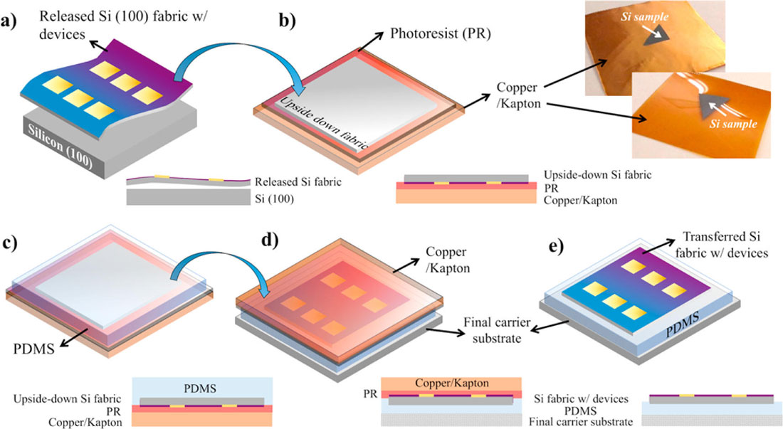
| 3D and 2D schematics describing the fabrication process flow of the double-transfer process of silicon (100) fabric onto a variety of asymmetric surfaces. (Reprinted with permission by American Chemical Society) (click on image to enlarge) | |
| "Our simple double-transfer process utilizes soft materials to integrate nonplanar FinFET and planar traditional MOSFET devices onto various wavy, curvilinear, irregular, or asymmetric surfaces, which helps to reduce the applied stress to the devices, and more importantly, assists to preserve performance with insignificant deterioration even at a bending state," Muhammad Mustafa Hussain, an Associate Professor of Electrical Engineering at King Abdullah University of Science and Technology (KAUST), who led the team, tells Nanowerk. "The use of a soft polymeric material gives us a way to not only provide a strong adhesion layer to reduce the strain and achieve more compliant systems but also encapsulate ultrathin, silicon fabric-based, flexible electronics." | |
| Jhonathan P. Rojas, first author of the paper, points out that this new technique offers the opportunity for large-area, full-die and even full-wafer transfer with ultra large-scale integration (ULSI) density capability. | |
| "This is a great example of how hetero-integration of diverse materials with different mechanical properties can work together to improve deployment and compatibility to all kinds of shapes, while retaining performance," he says. | |
| The team used a thin layer of PDMS as the flexible substrate to provide final adhesion and isolation from applied strains. PDMS has favorable mechanical and insulating properties and is biocompatible. Moreover, it is inexpensive, transparent, and stretchable. | |
 |
|
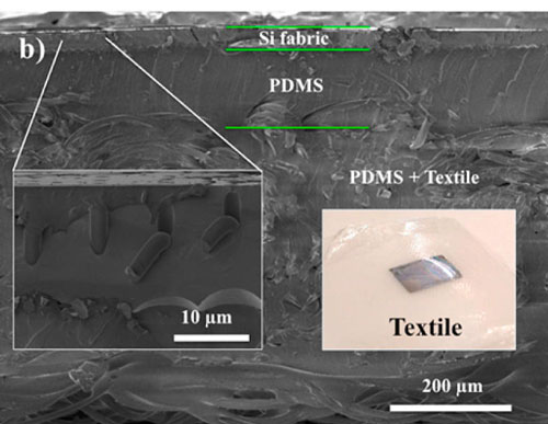
| Scanning electron microscope (SEM) image and optical image of released silicon sheets on textile. Inset in SEM shows zoomed-in versions and the formation of polymeric pillars formed during PDMS curing through the fabric's holes for increased grasp. (Reprinted with permission by American Chemical Society) | |
| Currently, the KAUST team is working on demonstrating more complex and faster circuitry to build high performing applications such as microprocessors and memory arrays, as well as system level implementations that include sensing, data processing, storage and communication as well as energy harvesting/management units. | |
| "We are also focusing on effective and automated ways to develop 3D integration of multiple silicon fabrics for multifunctional capabilities with extended area efficiency," notes Hussain. "There might be several scenarios where limited space and complex shapes are requiring electronics to have the ability to conformably adapt to such asymmetric forms in an area-efficient way, without compromising on electric performance. One advantage of our technique is that it can potentially enable 3D integration by allowing the stack of thin silicon sheets with devices, which remain high-performance and could be vertically interconnected." | |
 By
Michael
Berger
– Michael is author of three books by the Royal Society of Chemistry:
Nano-Society: Pushing the Boundaries of Technology,
Nanotechnology: The Future is Tiny, and
Nanoengineering: The Skills and Tools Making Technology Invisible
Copyright ©
Nanowerk LLC
By
Michael
Berger
– Michael is author of three books by the Royal Society of Chemistry:
Nano-Society: Pushing the Boundaries of Technology,
Nanotechnology: The Future is Tiny, and
Nanoengineering: The Skills and Tools Making Technology Invisible
Copyright ©
Nanowerk LLC
|
|
|
Become a Spotlight guest author! Join our large and growing group of guest contributors. Have you just published a scientific paper or have other exciting developments to share with the nanotechnology community? Here is how to publish on nanowerk.com. |
|