| Posted: Apr 17, 2009 | |
Nanoscale thermodynamics on the back of an envelope |
|
| (Nanowerk Spotlight) A recent study has shown that nineteenth century thermodynamics can still provide useful insights into twenty-first century nanosciences; and all this can be done with pencil and paper rather than an expensive super-computer! | |
| When the size of materials approaches the nanoscale, matter begins to behave highly exotically. By shrinking the size of materials, the surface-to-volume ratio increases. Considering this, scientists can study size effects on material properties from macroscopic laws, the so-called top-down approach. In thermodynamics, the Gibb's energy concept is particularly suited to describe the liquid-solid phase transition (what we mortals call the melting temperature). | |
| The above-mentioned study (Phase diagrams and optical properties of phosphide, arsenide, and antimonide binary and ternary III-V nanoalloys), published in the April 16, 2009 online edition of Physical Review B, has been developed by Dr. Gregory Guisbiers working at IEMN in Northern France, expresses the size-dependent relation determining the melting temperature and melting enthalpy of nanoparticles. In other words, his model allows the prediction of the melting temperature, energy bandgap and phase diagrams of semiconductors at the nanoscale." | |
| "Combining the nano-scale melting temperature with the bulk phase diagram equations, it has been possible to predict the phase diagrams of perfectly miscible nano-alloys," Guisbiers explains to Nanowerk. "Moreover, as the surface-to-volume ratio governs the size-dependent materials properties, size effects on the energy bandgap and the melting temperature are linked." | |
 |
|
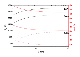
| Melting temperature (black) and energy bandgap (red) of gallium coumpounds versus the radius of spherical nanoparticles. (Image: Dr. Guisbiers, IEMN) | |
| In terms of applications, Guisbiers says that his model can be used to predict the energy bandgap of nano-semiconductors and to tune the thermo-optical properties of semiconductor nano-alloys especially those used in nano-optoelectronics applications. | |
| Before this work, phase diagrams of semiconducting nano-alloys were unknown at the nanoscale. But, says Guisbiers, by considering the surface energy concept, we can understand why nature – remember that nature always want to minimize energy – favors the element with the lowest surface energy on the nanostructure's surface. | |
| "This phenomena, called segregation, is responsible of the core-shell structure we generally see in nanostructures" says Guisbiers. "And as the melting temperature is lower for the element having the lowest surface energy, the surface melting phenomena can also be understood from nineteenth century thermodynamics." | |
 |
|
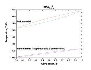
| Phase diagram of the InAsP for the bulk material and the spherical nanomaterial. The liquidus and solidus curves are indicated in red and green respectively for the bulk material. The liquidus and solidus curves are indicated in blue and purple respectively for the nanomaterial. (Image: Dr. Guisbiers, IEMN) | |
| Guisbiers' motivation for this study was that a large variety of material properties may be obtained by varying the size, shape and composition of the III-V elements involved in nano-alloys of these materials. | |
| "These alloys are used in systems for which they outperform silicon because of better-suited materials properties," says Guisbiers. "For example, the high electron mobility of gallium arsenide is advantageous in microwave devices and the small band gap of indium antimonide is suitable in infrared applications. Other systems as light-emitting diodes which require a well-tuned energy band gap can only be fabricated with semiconducting alloys." | |
| Arguing that material science at the nanoscale is a pre-requisite to nanotechnologies, Guisbiers says that nanomaterials' properties need to be determined theoretically and confirmed experimentally if possible before investigating complex nano-systems. He now plans to adapt his model to other materials properties such as the electrical ones. | |
 By
Michael
Berger
– Michael is author of three books by the Royal Society of Chemistry:
Nano-Society: Pushing the Boundaries of Technology,
Nanotechnology: The Future is Tiny, and
Nanoengineering: The Skills and Tools Making Technology Invisible
Copyright ©
Nanowerk LLC
By
Michael
Berger
– Michael is author of three books by the Royal Society of Chemistry:
Nano-Society: Pushing the Boundaries of Technology,
Nanotechnology: The Future is Tiny, and
Nanoengineering: The Skills and Tools Making Technology Invisible
Copyright ©
Nanowerk LLC
|
|
|
Become a Spotlight guest author! Join our large and growing group of guest contributors. Have you just published a scientific paper or have other exciting developments to share with the nanotechnology community? Here is how to publish on nanowerk.com. |
|