| Posted: Nov 17, 2006 | |
Nanotechnology in space: Carbon nanotubes harden electronics for use in aerospace |
|
| (Nanowerk Spotlight) The electrical properties of CNTs are extremely sensitive to defects which can be introduced during the growth, by mechanical strain, or by irradiation with energetic particles such as electrons, heavy ions, alpha-particles, and protons. When highly energetic particles collide, a latchup, electrical interference, charging, sputtering, erosion, and puncture of the target device can occur. Therefore the information on the effects of various types of high energetic irradiation on carbon nanotubes (CNTs) and other nanomaterials will be important in developing radiation-robust devices and circuits of nanomaterials under aerospace environment. As a result, degradation of the device performance and lifetime or even a system failure of the underlying electronics may happen. | |
| Researchers in South Korea conducted a systematic study of the effects of proton irradiation on the electrical properties of CNT network field effect transistor (FET) devices showing metallic or semiconducting behaviors. The most important outcome of this work is that no significant change in the electrical properties of CNT-based FET was observed, even after high-energy proton beam irradiated directly on the device. This result show that CNT-based devices can be a promising substitute for classical silicon-based devices, which are known to be very fragile against proton radiations. | |
| It has been reported previously that electronic devices became more radiation tolerant when their dimensions are reduced.For example, multi-quantum well or quantum dot devices can be tens or hundreds times more radiation tolerant than conventional bulk devices. It even was shown that quantum dot/CNT-based photovoltaic devices were five orders of magnitude more resistant than conventional bulk solar cells. | |
| "Although there have been many reports on the potential utilizations in aerospace environment, as far as we know, ours is the first study that the CNT-electronic devices can be used to overcome ever-lasting fragility of the silicon-based devices in highly harmful nature" Dr. Takhee Lee describes the core finding of the study to Nanowerk. | |
| Recently, a few studies on radiation effects of high energetic particles such as proton, electron, and heavy ions on nanomaterials like CNTs and nanowires have focused on the changed structural properties of the nanomaterials after irradiation. Lee, who is an Assistant Professor in the Department of Materials Science and Engineering at Gwangju Institute of Science and Technology (GIST) in South Korea, and his colleagues went one step further: They systemically investigated the nature and extent of damage caused by proton radiation on real electronic devices fabricated with single walled carbon nanotubes (SWCNT). | |
 |
|
| Images of the CNT network-FET used in the study. (Source: Dr. Lee) | |
| "Having a research background in nanoelectronics devices, I asked myself what will happen if actual nanoelectronics devices are exposed to high energy radiation" Lee says. "Then, I formed a group of experts, including Prof. Kwanwoo Shin at Sogang University, who has been working on material properties under high energy radiation. Initially, we were looking for a method to modifying the physical and chemical properties of carbon nanotubes by introducing structural defects with high energetic proton radiation. Surprisingly, we found out that our CNT network transistors were quite robust under the radiation. Even when we increased the energy and radiation time, the results showed consistent radiation-hardness." | |
 |
|
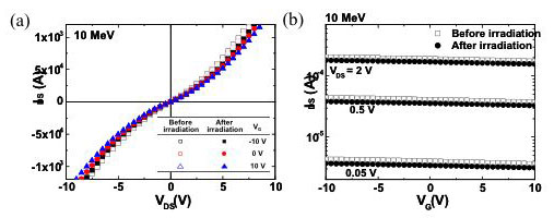
| Transfer characteristics of metallic SWNT network FETs before and after proton irradiation at 10 MeV and a fluence of 1.4 x 1012 cm-2. (a) Source–drain current versus drain voltage at various gate voltages (VG = -10, 0, and 10 V). (b) Source–drain current as a function of gate voltage at various source–drain biases (VDS = 0.05, 0.5, and 2 V). (Source: Dr. Lee) | |
| In their experiments, CNT-FET devices using single-walled CNTs were exposed to 10–35 MeV proton beams with a fluence of 4 x 10¹⁰-4 x 1012 cm-2 that are comparable to the aerospace environment. None of the 26 SWNT network FET devices that were fabricated for the experiments exhibited any significantly altered electrical changes before and after proton irradiation. | |
| "These results indicate a certain radiation hardness of CNT-based electronic devices under proton irradiation in our exposure conditions and suggest that the CNT devices are promising for future application in aerospace" says Lee. | |
| Having studied proton radiation effects on CNT networks, Lee and his colleagues are currently working on other radiation sources, covering entire magnetosphere spectrum, a flux of energetic electrons, UV-Ozone, and heavy ions. | |
| "We believe that this series of experiments will eventually confirm whether CNT-based electrical devices can be used as a substitute of the classical devices in aerospace" Lee says. "Of cause, if we could reach a collaboration with NASA, the ultimate solution for this will be to actually send the samples into space and measure the radiation effects. For now, we mimic the space environment in lab facility." | |
| Lee is convinced that, in future, nanotubes and nanomaterials will be used as a major component of various space applications and devices, including coating layers, radiation shielding, and electronic components in space shuttles or space stations. | |
| Lee sees much work to be done and hopes other researchers will work in this area "We still need more fundamental understanding on CNT materials under high energy irradiation, in terms of the physics behind it. Since this research area is in its infancy, we hope that many more researchers will look into the potentials of this research, and study physical, chemical, mechanical, electrical properties of nanomaterials under the radiations." | |
| These findings are reported in a recent paper in Nanotechnology ("Radiation hardness of the electrical properties of carbon nanotube network field effect transistors under high-energy proton irradiation"). | |
 By
Michael
Berger
– Michael is author of three books by the Royal Society of Chemistry:
Nano-Society: Pushing the Boundaries of Technology,
Nanotechnology: The Future is Tiny, and
Nanoengineering: The Skills and Tools Making Technology Invisible
Copyright ©
Nanowerk LLC
By
Michael
Berger
– Michael is author of three books by the Royal Society of Chemistry:
Nano-Society: Pushing the Boundaries of Technology,
Nanotechnology: The Future is Tiny, and
Nanoengineering: The Skills and Tools Making Technology Invisible
Copyright ©
Nanowerk LLC
|
Become a Spotlight guest author! Join our large and growing group of guest contributors. Have you just published a scientific paper or have other exciting developments to share with the nanotechnology community? Here is how to publish on nanowerk.com.