| Posted: Jun 18, 2009 | |
Nanotechnology structuring of materials with atomic precision |
|
| (Nanowerk Spotlight) The manifold properties of carbon nanotubes (as well as other carbon nanomaterials such as fullerenes and graphene) are related to the various ways the carbon atoms can be arranged to form the tube lattice. Studies have shown that atomic-scale defects in these lattices can strongly influence the electronic and mechanical properties of the nanotubes. The simplest defect type is a vacancy where an atom is missing from the lattice site. Such defects can also be seen as chemically active sites for tube side wall functionalization. Due to the difficulty of observing vacancies directly, it remained unclear under what conditions vacancies in nanotubes are stable or exist at all. | |
| "To study the behavior of the nanotube lattice upon the removal of single atoms, it would be necessary to create vacancies in predefined positions and to observe the relaxation of the lattice around these sites at the same time and with atomic resolution," Florian Banhart explains to Nanowerk. "'This is an experimental challenge and might also be used to tailor the properties of nanotubes by creating defects locally and to obtain devices with a desired function." | |
| Banhart, a Professor of Physics at the University of Strasbourg in France, together with Julio A. Rodriguez-Manzo, a postdoc researcher in his group, have now demonstrated a technique that allows them to remove carbon atoms from carbon nanotubes with atomic precision and in a controlled way with an extremely focused electron beam. | |
| "In our in situ electron microscopy experiment we see the response of the nanotube to the the creation of vacancies" says Banhart. "This is an important issue because the outstanding physical properties of carbon nanotubes (electrical conductivity, resistance against mechanical failure etc.) depend sensitively on the presence of defects such as vacancies. Our studies in a wide range of specimen temperatures showed several unexpected phenomena." | |
| The two scientists also found that the behavior of single- and double-wall nanotubes upon the removal of atoms is quite different. Vacancies in single-wall tubes can be generated by the beam, but are unstable and vanish immediately by a reconstruction of the graphenic lattice. In double-wall tubes, however, vacancies are stable due to interlayer bonds in the tubes and visible up to a certain temperature. | |
| Banhart and Rodriguez-Manzo describe their findings in a recent edition of Nano Letters ("Creation of Individual Vacancies in Carbon Nanotubes by Using an Electron Beam of 1 Å Diameter"). | |
| For their experiments, they used a novel scanning transmission electron microscope (STEM) with an aberration corrector. The instrument allows to focus an extremely intense electron beam with one Ångstrom diameter onto the object. This way not only can images of nanostructures be obtained with real atomic resolution but also irradiation experiments can be carried out on the scale of an interatomic distance. | |
 |
|
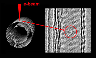
| A model of the experiment is on the left and a scanning transmission electron microscopy image of a vacancy in a double-wall carbon nanotube on the right. (Image: Dr. Banhart, Université de Strasbourg) | |
| Besides being the first atomic-scale study of carbon nanotubes in a STEM, this study is also the first showing the generation of individual point defects with an Ångstrom-size electron beam. With the upcoming availability of STEMs with Ångstrom resolution, this study could have a considerable impact in the field of atomic-scale structuring of materials. | |
| The structuring of materials with sub-nanometer precision is a challenge in nanotechnology. Until now, just surface atoms have been moved with the tips of scanning tunneling microscopes (STM) or atomic force microscopes (AFM). By using electron beam structuring, scientists can now apply this technique to the interior of materials (the electron beam penetrates small objects). | |
| Banhart's work was undertaken to observe and understand defect formation in carbon nanotubes. The resulting findings shed light on how nanotubes change their structure upon generation of defects. Furthermore, the application of a focused electron beam might also show a route towards nanotechnology engineering of nanotubes or other nanomaterials for specific applications: | |
| "Our study shows how the irradiation of nano objects with a focused electron beam can be used to tailor the objects with almost atomic precision," says Banhart. "The technique can now be applied to the atomic-scale structuring of other materials." | |
 By
Michael
Berger
– Michael is author of three books by the Royal Society of Chemistry:
Nano-Society: Pushing the Boundaries of Technology,
Nanotechnology: The Future is Tiny, and
Nanoengineering: The Skills and Tools Making Technology Invisible
Copyright ©
Nanowerk LLC
By
Michael
Berger
– Michael is author of three books by the Royal Society of Chemistry:
Nano-Society: Pushing the Boundaries of Technology,
Nanotechnology: The Future is Tiny, and
Nanoengineering: The Skills and Tools Making Technology Invisible
Copyright ©
Nanowerk LLC
|
|
|
Become a Spotlight guest author! Join our large and growing group of guest contributors. Have you just published a scientific paper or have other exciting developments to share with the nanotechnology community? Here is how to publish on nanowerk.com. |
|