| Posted: Jun 25, 2009 | |
Observing carbon nanotubes can damage them - even at 80 kV |
|
| (Nanowerk Spotlight) A few days ago we ran a Nanowerk Spotlight ("Nanotechnology structuring of materials with atomic precision") on a nanostructuring technique that uses an extremely narrow electron beam to knock individual carbon atoms from carbon nanotubes with atomic precision, a technique that could potentially be used to change the properties of the nanotubes. In contrast to this deliberately created defect, researchers are concerned about unintentional defects created by electron beams during examination of carbon nanomaterials with transmission electron microscopes like a high-resolution transmission electron microscope (HRTEM). | |
| For a long time it has been thought that if the accelerating voltage of electrons could be reduced to 80 kV in an electron microscope, then the electrons would not possess sufficient energy to cause knock-on damage in carbon nanomaterials. Knock-on damage occurs when electrons are scattered by the nucleus of the atom they are probing. Upon scattering, energy is transferred. In some circumstances this energy can be large enough to dislodge the atom from its position. | |
| A British-German team has examined how electrons accelerated at 80 kV interact with singe-walled carbon nanotubes (SWCNTs) and shown that in some circumstances SWCNTs were unstable. | |
| "We investigated this using a state-of-the-art transmission electron microscope fitted with spherical aberration correctors," Jamie Warner explains to Nanowerk. "This allowed us to see the atomic structure in the carbon nanotubes and determine their chirality. We observed carbon nanotubes that were contaminated with material on the outside were not stable under the electron beam. We also observed that carbon nanotubes with defects in their atomic structures were not stable in the electron beam." | |
| Furthermore, the team found that the stability of nanotubes under 80 kV electron beam irradiation was also linked to their diameter, with smaller nanotubes more unstable. This is related to the increase in strain in the carbon bond with increase in curvature. Thus small nanotubes have higher curvature and more bond strain. | |
 |
|
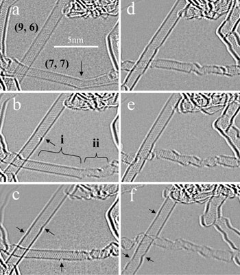
| Time series of HRTEM images showing the rapid destruction of a (7,7) SWCNT with defects compared to the defect-free (9,6) SWCNT. (Reprinted with permission from American Chemical Society) | |
| These findings have been published in a recent online edition of ACS Nano ("Investigating the Diameter-Dependent Stability of Single-Walled Carbon Nanotubes"). | |
| Warner, first author of the paper, is the Violette and Samuel Glasstone Research Fellow in Science in the Department of Materials at the University of Oxford. He worked with colleagues from IFW Dresden, Germany, and the Department of Engineering at the University of Cambridge. | |
| This work proves to be valuable to other researchers in the field because it provides a detailed study on what they need to be careful of when examining their samples in the electron microscope. Prior to this work, there has not been a detailed study of the effects of electron beam irradiation on nanotubes with different diameters, cleanliness and structural quality. Now, researchers will be able to determine the chirality of their carbon nanotubes using conditions that will not damage the tube. They now have a guideline of the care that is necessary to avoid structural reconfiguration. | |
| Warner points out that it is important to be able to distinguish between intrinsic structure of the material, and changes induced by the electron beam. | |
| "Transmission electron microscopy is an excellent tool for determining the atomic structure of carbon nanotubes, but we do not want to modify the properties if the structure is to be used in further applications" he says. "We hope that our study sheds light on the delicate care that is required to image carbon nanotubes in order to determine their chirality without inducing structural changes." | |
| In their experiments, the scientists showed that SWCNTs contaminated with large amounts of dirt/material on the outside were unstable. When only trace amounts of nanocarbon was present on the surface of larger 3 nm diameter SWCNTs, it was incorporated into the side walls of the SWCNTs after prolonged electron beam irradiation. | |
| Warner notes that SWCNTs with significant defects were unstable and degraded faster than pristine SWCNTs and that they found that the stability of SWCNTs increases with increasing diameter – results which correlate well with the theoretical calculations involving SWCNTs under electron beam irradiation. However, SWCNTs with diameters below 1 nanometer appear to be very prone to electron beam induced structural damage. In larger 2-3 nm diameter SWCNTs, defects were mobile and in some cases only lasted temporarily. | |
| "Most importantly, although it has long been thought that 80 kV might be below the knock-on damage threshold for SWCNTs, we find electron beam irradiation still produces defects in pristine SWCNTs resulting in damage," says Warner. "However, the beam current densities we used were large and excessive, and by lowering this, damage may be avoided for sufficiently long periods of time." | |
| The research team emphasize that their results indicate that extreme care must be taken when performing in situ HRTEM chirality determination of SWCNTs in applications such as FET devices where damage to the structure is unwanted. | |
| According to Warner, the major challenge is to continue to reduce the accelerating voltage in transmission electron microscopes equipped with spherical aberration correctors. "It is necessary to have the correctors, as they enable high spatial resolution to image the atomic structure. There is interest to get to as low as 20 kV accelerating voltages in order to image small organic molecules." | |
 By
Michael
Berger
– Michael is author of three books by the Royal Society of Chemistry:
Nano-Society: Pushing the Boundaries of Technology,
Nanotechnology: The Future is Tiny, and
Nanoengineering: The Skills and Tools Making Technology Invisible
Copyright ©
Nanowerk LLC
By
Michael
Berger
– Michael is author of three books by the Royal Society of Chemistry:
Nano-Society: Pushing the Boundaries of Technology,
Nanotechnology: The Future is Tiny, and
Nanoengineering: The Skills and Tools Making Technology Invisible
Copyright ©
Nanowerk LLC
|
|
|
Become a Spotlight guest author! Join our large and growing group of guest contributors. Have you just published a scientific paper or have other exciting developments to share with the nanotechnology community? Here is how to publish on nanowerk.com. |
|