| Posted: Jul 01, 2009 | |
Nanoarches advance nanotechnology's tool box |
|
| (Nanowerk Spotlight) One of the ultimate goals of nanotechnology is to fabricate functional devices at the nanoscale. A nanodevice is expected to integrate components of different material compositions and geometries. The integration is likely to be carried out on silicon if information processing is required. Thus far, the basic building blocks for nanodevices are nanoparticles, for which there are many material candidates; and nanotubes, for which the candidates are fewer (they are mostly carbon, although non-carbon based tubes have been fabricated as well). One-dimensional (1-D) nanomaterials such as nanotubes are useful for component connection and for the transport of charge, heat and vibration. | |
| In addition to the limited material selection, common 1-D nanomaterials are usually straight. Composite 1-D nanomaterials are rarer. Often they are also produced as discrete and unorganized units (although there are vapor phase methods to grow straight nanotube arrays on certain surfaces). | |
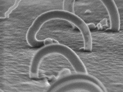
| Scientists in Singapore have now successfully fabricated a family of aligned one-dimensional C-curved nanoarches of different compositions by a simple and scalable method for the first time. | |
 |
|
| Aligned 1-D C-curved nanoarches of CNT encapsulating crystalline tin nanorods. (Reprinted with permission from American Chemical Society) | |
| "Our nanoarches are actually nanotubes with their extremities firmly attached to the silicon surface, thereby forming a turned letter C," Jim Yang Lee explains to Nanowerk. "We have also developed a new methodology for synthesizing tin oxide nanotubes using in situ formed carbon nanotubes as the active template. Our fabrication method is generic and could, in principle, be applied to the preparation of other aligned 1-D nanomaterials." | |
| Lee is a professor in the Department of Chemical & Biomolecular Engineering at the National University of Singapore (NUS). Together with his PhD student Da Deng he has published his research results in a recent online edition of ACS Nano ("A Family of Aligned C-Curved Nanoarches"). | |
| While the main motivations for this work was to achieve surface wettability control by structuring the silicon wafer surface with different nanostructures, Lee's team is also interested in using the nanoarches as nanoscale component connectors. | |
| According to Lee, in the design of nanodevices there may be a need to align 1-D nanostructures of the desired curvature and composition on a substrate to provide efficient transport of electrons or for optical and thermal excitations. "Our study demonstrates one example of the enabling methodology" he says. "The family of C-curved nanoarches that we have shown can also provide 3-D connectivity, which may be more advantageous than linear 1-D connectivity in certain cases. Such 3-D connections may eventually find applications in the construction of nanoscale sensors, transducers, and transponders." | |
| Lee points out that the 1-D nanotubes with curvatures, such as the nanoarches, are more strain-tolerant and add flexibility to connectivity. "The nicest thing of all is perhaps that they can be made from different materials conductivities – carbon nanotubes, tin oxide nanotubes, and tin nanorods in carbon nanotubes – and assembled on the silicon surface by a simple chemical method," he says. "We used the assembly for silicon wettability control but there may be more exciting applications out there." | |
| There are still some challenges to overcome with this novel technique, in particular density and positioning control, i.e. putting down a sufficient number of nanoarches at specific locations. Lee is confident that these can in principle be solved through careful scoping of the experimental variables or perhaps a combination of lithographic techniques and their method. | |
| While the NUS team has only tested the nanoarches for silicon surface wettability control, the very different electronic properties of the materials that can be used to fabricate the nanoarches – from conductors (CNTs) to semiconductors (tin oxide nanotubes) to superconductors (tin nanorods in CNTs) – may be useful in designing components for some future nanodevices. | |
| Consequently, Lee and his group are planning to study these nanoarches as connectors for nanodevices and how they can be integrated with material components with specific functions. "Unfortunately we do not yet have the tool sets for manipulating the nanoarches at the nanoscale level, but we are working on that" says Lee. | |
 By
Michael
Berger
– Michael is author of three books by the Royal Society of Chemistry:
Nano-Society: Pushing the Boundaries of Technology,
Nanotechnology: The Future is Tiny, and
Nanoengineering: The Skills and Tools Making Technology Invisible
Copyright ©
Nanowerk LLC
By
Michael
Berger
– Michael is author of three books by the Royal Society of Chemistry:
Nano-Society: Pushing the Boundaries of Technology,
Nanotechnology: The Future is Tiny, and
Nanoengineering: The Skills and Tools Making Technology Invisible
Copyright ©
Nanowerk LLC
|
|
|
Become a Spotlight guest author! Join our large and growing group of guest contributors. Have you just published a scientific paper or have other exciting developments to share with the nanotechnology community? Here is how to publish on nanowerk.com. |
|