| Posted: Sep 08, 2009 | |
Nanotechnology researchers add fast laser printing to their nanofabrication tool box |
|
| (Nanowerk Spotlight) A few years ago it was discovered that the process of thermal inkjet printing can be applied to fabricate hard tissue scaffolds (such as bones) and, just recently, soft tissue with liquid biomaterials. Research is also underway to use inkjet printing for the fabrication of organic semiconductors, opening a route to the fabrication of high-performance and ultra low-cost electronics such as transparent electronics and thin film solar cells (see for instance: "Desktop printing with nanotube ink"). As a matter of fact, the installation of the world's first silicon-ink based solar cell pilot production was completed this January. | |
| In your office, though, you have a choice between inkjet printers and (usually much faster) laser printers. And soon, nanotechnologists might have this choice, too. Researchers in California have demonstrated a novel technique – which they call Nanoparticle Pen, or NanoPen for short – for rapidly 'printing' various nanoparticles such as gold nanoparticles, carbon nanotubes, and semiconducting and metallic nanowires, on a photoconductive surface by light, much like a laser printer prints toner powder on paper. | |
| "NanoPen introduces a flexible, real-time reconfigurable, and large-scale method for patterning various nanostructures with potential applications in chemical and biological sensing, opto- and nanoelectronic device fabrication, nanostructure synthesis, and photovoltaics," Ming Wu tells Nanowerk. "This mechanism requires very low optical power density and as a result we can use a low-cost digital projector for printing. Compared with other nanoparticle patterning techniques, the NanoPen is based on projection of the entire optical image, and is faster than the serial writing of scanning probe based approaches." | |
| Wu is professor of Electrical Engineering and Computer Sciences, and Co-Director of Berkeley Sensor and Actuator Center (BSAC) at the University of California, Berkeley. Together with his team he reports the novel use of an optoelectronic tweezers platform for directly and permanently writing patterns of nanoparticles in a recent issue of Nano Letters (NanoPen: Dynamic, Low-Power, and Light-Actuated Patterning of Nanoparticles) | |
 |
|
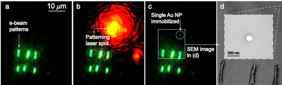
| Immobilization of a single 90 nm diameter gold nanoparticle. (a) Pre-designated target patterns were fabricated on the OET device using e-beam lithography. (b,c) Once the laser spot is positioned, a nanoparticle is attracted and patterned on the surface, ∼10 µm above the e-beam pattern. (d) SEM image of the area indicated in (c) by the white rectangle, showing the patterned nanoparticle near the e-beam structure. The inset is a zoom-in SEM image of the particle. (Reprinted with permission from American Chemical Society) | |
| The Berkeley scientists point out that researchers have already developed several different techniques for producing patterns of nanoparticles but several limitations prevent widespread application of these techniques – they tend to be too complex and slow, requiring bulky instrumentation and taking minutes or even hours to complete. These techniques also require the use of very high temperatures to apply the nanostructures to their target surfaces. | |
| "Optical tweezers are the most widely known optical manipulation technique" explains Wu. "However, they require very high optical power density – often at the level of vaporizing tiny nanoparticles. This motivated us to investigate alternative optical manipulation techniques. As a result, our NanoPen reduces the optical density by three to four orders of magnitude." | |
 |
|
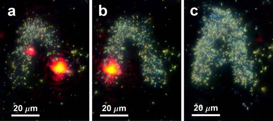
| NanoPen patterning of semiconducting (Silicon) nanowires. (a-c) The process of patterning Silicon nanowires in the form of character (?A?) using the NanoPen technique. The Silicon nanowires have ∼100-200 nm diameters and are ∼5-20 µm in length. (Reprinted with permission from American Chemical Society) | |
| It appears that the NanoPen solves this problem. Note that the name NanoPen refers to a method for patterning nanoparticles and does not mean nanoscale positioning accuracy. | |
| "In our lab we used it to deposit various nanoparticles into specific patterns in the presence of relatively low light and temperature intensities," says Wu. "The process, which requires the use of special photoconductive surfaces, takes only seconds to complete. Manufacturers can adjust the size and density of the patterns by adjusting the voltage, light intensity, and exposure time applied during the process." | |
| Applications of patterned nanostructures range from fabrication of opto- and nanoelectronic devices in the case of nanowires and carbon nanotubes to DNA microarrays depending on the type and characteristics of the patterned nanoparticles. Wu's team has already used NanoPen to pattern densely packed gold nanoparticles for surface-enhanced Raman spectroscopy (SERS). SERS is well-known for its capability to measure the 'fingerprints' of chemical and biological molecules with pico-molar sensitivities. NanoPen provides a fast prototyping capability to produce arrays of SERS probes. | |
| "One area that we haven't explored yet is using NanoPen for patterning biomaterials such as DNA and proteins" says Wu. "Patterning of such biomaterials integrated with microfluidics has potential applications in creation of DNA microarrays and that's something we'll look into during future investigations." | |
 By
Michael
Berger
– Michael is author of three books by the Royal Society of Chemistry:
Nano-Society: Pushing the Boundaries of Technology,
Nanotechnology: The Future is Tiny, and
Nanoengineering: The Skills and Tools Making Technology Invisible
Copyright ©
Nanowerk LLC
By
Michael
Berger
– Michael is author of three books by the Royal Society of Chemistry:
Nano-Society: Pushing the Boundaries of Technology,
Nanotechnology: The Future is Tiny, and
Nanoengineering: The Skills and Tools Making Technology Invisible
Copyright ©
Nanowerk LLC
|
|
|
Become a Spotlight guest author! Join our large and growing group of guest contributors. Have you just published a scientific paper or have other exciting developments to share with the nanotechnology community? Here is how to publish on nanowerk.com. |
|