| Posted: Sep 09, 2009 | |
Library of 'nanobits' makes for a flexible 3D nanotechnology construction kit |
|
| (Nanowerk Spotlight) The folks at the European NanoHand project, whose nanogripper design we have covered in a previous Nanowerk Spotlight (Nanotechnology gets a grip), seem to have loved playing with their plastic toy kits as kids. At least that's the impression you get when watching their latest video explaining their proof-of-principle study of scanning probe tips defined by planar nanolithography and integrated with AFM probes using nanomanipulation: | |
| "We have prefabricated nanoscale needles, to be picked up by nanogrippers inside a scanning electron microscope" Peter Bøggild tells Nanowerk. "We then use these nanobits as ultralong tips in atomic force microscopes (AFM). We call the needles 'nanobits' because they remind us of drill bits – you can have a library of different nanobits and then pick the one you want, and mount it where you want it." | |
| Bøggild is an associate professor and leader of the Nanointegration Group at the Department of Micro and Nanotechnology at the Technical University of Denmark (DTU). | |
| Working with colleagues from the University of Oldenburg in Germany, the researchers have published their findings in the September 2, 2009 online edition of Nanotechnology ("Nanobits: customizable scanning probe tips"). | |
| In their work, the team chose an approach that involves fabricating arrays of flake-like tips – these nanobits are 2–4 µm long and 120–150 nm thin flakes of silicon dioxide or silicon nitride – by planar electron beam nanolithography for selection, detachment and assembly on standard pyramidal AFM probes by direct manipulation. | |
 |
|
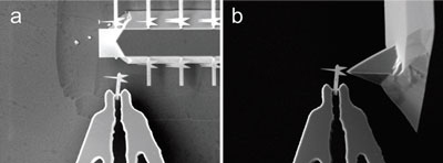
| Integration of a nitride nanobit with an AFM probe using a topology optimized microgripper. (a) Gripper detaching a nitride nanobit. (b) Gripper holding a nanobit while approaching an AFM probe. (Reprinted with permission from IoP Publishing) | |
| "The advantage of our approach is a considerable freedom in defining the size, shape and even material to meet the requirements of specific applications," explains Bøggild. "Since the tips are batch fabricated with electron beam lithography, thousands of tips with different combinations of size and shape of the end-effector can be fabricated at no extra effort, creating large libraries of tip shapes to choose from." | |
| He mentions out that their experiments showed that standard AFM scanning methods can easily be applied using the nanobit-enhanced probes. "Using other end-effector shapes more sophisticated experiments such as scanning of sidewall structures or even non-planar AFM scanning can be realized". | |
| "We believe that this technique has powerful perspectives" says Bøggild. "Since we can pretty much make the 'connectors' anywhere in any material we like, and since we can define the 'nanobits' freely, I think it is the first demonstration of something done with 3D nanomanipulation that cannot be realized with any other technique." | |
| He also points out that while nanolithography gives full freedom in two-dimensional design, but is very limited in the third dimension, nanomanipulation takes the finished 2D structures and turn them 90 degrees – making it possibility to fabricate 3D structures out of plane nanolithographic structures. | |
| By the way, for 'techies' among you, the team has also posted a longer video that explains in some more detail how the semi-automatic robot assembly system 'NanoLab' works: | |
| "The system, NanoLab, is actually pretty cool" says Bøggild, "it uses image recognition to guide the grippers to the nanotubes, and can do the assembly fully automatic.It also has mobile robots – like small cm sized tanks with robot arms (made by EPFL in Lausanne), and a tiny gripper at the end. I'm kind of amazed this unlikely approach turned out to be the one that worked." | |
| The NanoHand projects ambitiously aims at not just making nanoassembly possible, or facilitate nanoassembly, but actually build equipment and methodology that does nanoassembly, i.e. to build a prototype nano-assembly line (read more about NanoHand here: Sticky fingers? Tiny robots to grip nanotubes). | |
 By
Michael
Berger
– Michael is author of three books by the Royal Society of Chemistry:
Nano-Society: Pushing the Boundaries of Technology,
Nanotechnology: The Future is Tiny, and
Nanoengineering: The Skills and Tools Making Technology Invisible
Copyright ©
Nanowerk LLC
By
Michael
Berger
– Michael is author of three books by the Royal Society of Chemistry:
Nano-Society: Pushing the Boundaries of Technology,
Nanotechnology: The Future is Tiny, and
Nanoengineering: The Skills and Tools Making Technology Invisible
Copyright ©
Nanowerk LLC
|
|
|
Become a Spotlight guest author! Join our large and growing group of guest contributors. Have you just published a scientific paper or have other exciting developments to share with the nanotechnology community? Here is how to publish on nanowerk.com. |
|