| Posted: Oct 06, 2009 | |
Strain engineering graphene's transport |
|
| (Nanowerk Spotlight) Researchers at Boston University have found that local deformations in a graphene sheet can strongly influence electron flow across the system, causing suppression of conductance at low densities, and making electrons behave as if they were living in a nanoribbon or quantum dot. All this without cutting the graphene sheet, which opens the prospect towards a reversible and controllable transport gap in monolayer graphene via strain engineering. | |
| Graphene is an impressive condensed matter system that, to all appearances, never ceases to impress and challenge our entrenched intuitions regarding solid state systems. For the most part, graphene's perceived (and proven) versatility as an electronic system, and the vast array of applications that are now seen as graphene promises, stem from the simple fact that graphene is a membrane. In other words, graphene is a highly atypical electronic system in that it consists of nothing but a surface. Therefore "bulk" properties (like its intrinsic bandstructure that derives from the arrangement of the carbon atoms) and surface effects are destined to be intimately connected. | |
| This simple fact, no matter how obvious it might seem, begs a considerable revision of our mindset when it comes to exploring the large potential of graphene for electronics applications. Traditional condensed matter systems are what is called "bulk" materials. Their properties derive directly from the type and arrangement of their atoms. | |
| In many ways the physicist, and later the engineer, is a prisoner of the material itself: nature gives us materials with definite "bulk" properties (definite arrangements of atoms, definite bandstructures, definite transport characteristics, etc.), and those properties are dictated inexorably by nature. But, as it turns out, nature-given compounds are often rather dull for the demands of current electronics applications. | |
| To circumvent the constraints imposed by nature we commonly resort to certain tricks, like combining different materials, creating alloys or more complex compounds, mixing-in selected impurities, or stacking different compounds into nanostructured end-materials. | |
| At any rate, even then, once the recipe is fine tuned to yield a material with certain suitable characteristics, one is still prisoner of the material: its properties cannot be altered, and how a certain device will behave is, one can say, written in stone. This arises precisely because the properties in question are "bulk" properties, and it is near to impossible to change them without creating a new material altogether. | |
| This is one of the dimensions where graphene has a tremendous advantage. By lacking the bulk between its two surfaces, graphene lends itself to avenues of exploration that are forbidden in traditional materials research. One such avenue is chemical modification of graphene's surface. A graphene sheet can be seen as a macroscopic molecule made of carbon, which turns out to be the most flexible element in nature (organic chemistry derives its richness from this chemical flexibility of carbon). | |
 |
|
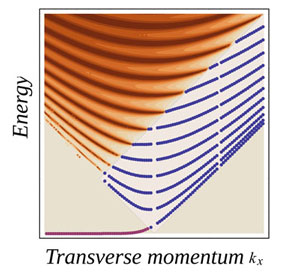
| Figure 1: The discrete spectrum that arises in the region under local strain. The energy scales are the same as the ones in a conventional nanoribbon, yielding energy gaps of Eg ≈ 1eV/L(nm), where L is the length of the strained region. (Image: Vitor M. Pereira and Antonio Castro Neto. Boston University) | |
| It is plain to see that there is a whole unexplored world around chemical tailoring of graphene (see: "Graphene: Calling all chemists"), both because graphene is made of carbon, and because, being a surface, is totally exposed to the environment. Early steps have already been taken in the direction of functionalized graphene structures, like graphene oxide ("Chemical methods for the production of graphenes") or hydrogenated graphene ("Control of Graphene's Properties by Reversible Hydrogenation: Evidence for Graphane"). | |
| Another avenue still much unexplored is the interplay between elastic response of graphene and its electronic and transport characteristics. Whereas graphene exhibits a tremendous in-plane Young modulus that makes graphene the strongest material ever measured ("Measurement of the Elastic Properties and Intrinsic Strength of Monolayer Graphene"), it is, simultaneously, a very soft membrane when it comes to displacements in the third spacial direction. | |
| In a recent work published in Physical Review Letters ("Strain Engineering of Graphene?s Electronic Structure"), Vitor M. Pereira and Antonio Castro Neto (Boston University) have shown how these two seemingly independent aspects of elasticity and electronic/transport properties are in fact intertwined, and might be used to explicitly tune the electronic response of graphene in a reversible way. | |
| The synthesis of graphene brought about the emergence of a new concept in condensed matter: the prospect of a tunable bandstructure. From the above considerations, conventional materials have their immutable, nature-given bandstructure. | |
| The ultimate quest in current graphene research centers around the best technique to induce a transport gap in monolayer graphene, which is otherwise a zero-gap semiconductor. If such gap can be afterwards tuned on demand so much the better. | |
| Current focus lies upon finite-size quantization in nanostructured, like nanoribbons or quantum dots. These structures involve nanopatterning of graphene sheets, which tends to introduce unintended disorder and roughness in the resulting nanostructures, which would be detrimental for the performance of graphene-based devices. In contrast to this "paper cutting" route, Pereira and Castro Neto propose an "origami" approach, based upon strain engineering. | |
| It is known that a bulk spectral gap cannot be induced in graphene by just stretching ("A tight-binding approach to uniaxial strain in graphene") (at least within reasonable amounts of strain). This is a consequence of symmetry, which protects the Diracness of the low energy fermions in graphene. | |
| Nevertheless, Pereira and Castro Neto found that local strain profiles can be suitably tailored to alter the conducting properties of graphene, resorting only to small deformations of the carbon lattice. A Dirac electron dashing throughout graphene will feel a local deformation as a tunneling barrier. Not all incidence angles are allowed to penetrate that region and this suppresses electronic flow. There are several consequences of this, which can be used to collimate electrons in graphene systems, or to filter electrons with certain velocities. | |
| But most interesting is the fact that this suppression of electron flow can lead to a transport gap that depends on the amount of local strain. Moreover, inside the locally deformed regions, the electrons behave as if they were spatially quantized in an effective nanoribbon (Fig. 2). In other words, local strain can generate the same features that are seen in graphene nanoribbons, except that one doesn't need to cut them, and the process can be reversed, on demand, by relieving the applied strain. | |
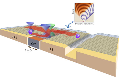
| These results are particularly motivating because we are now seeing the first experiments that try to address and control the interplay between strain and transport in graphene sheets. For example, in January we saw the first investigations of effects of controlled strain on the electronic resistivity of graphene ("Large-scale pattern growth of graphene films for stretchable transparent electrodes"); and over the summer researchers at U. C. Riverside have reported control over rippling in suspended graphene membranes ("Controlled ripple texturing of suspended graphene and ultrathin graphite membranes"). This makes the prospect of electronic structures tunable via strain engineering, as proposed by Pereira and Castro Neto, a more tangible reality. Structures could be made by tailoring spatially heterogeneous substrates, with different thermal expansion coefficients in different regions, such that variations in temperature would generate the needed local strain profiles Alternatively, one could also explore the impermeability of graphene, and trap gases in trenches or holes suitably carved in substrates. By tuning temperature or pressure the trapped gases would locally inflate the graphene sheet and, again, induce local strain. | |
 |
|
| Figure 2: Depiction of a a possible setup that induces local strain. A substrate is fabricated out of two materials with different thermal expansion coefficients (α1, α2), or containing selected trenches. Any change in temperature will cause a different amount of linear expansion, such that the two regions of graphene above are deformed by different amounts. This generates local strain, which will scatter the Dirac electrons propagating across that region. This creates a transport gap in the conductance at low densities. At the same time, for a range of incoming velocities, the electrons can become confined, just exactly as in a nanoribbon. (Image: Vitor M. Pereira and Antonio Castro Neto. Boston University) | |
| The possibilities are even more amplified when we realize that strain directly influences the chemical reactivity of graphene, such that the strain and chemical routes are not exclusive, but complementary. | |
| As A. K. Geim writes in his last review article ("Graphene: Status and Prospects"): "Research on graphene's electronic properties is now matured but is unlikely to start fading any time soon, especially because of the virtually unexplored opportunity to control quantum transport by strain engineering and various structural modifications." | |
| All this seems to indicate that strain engineering – exploring the interplay between graphene's elastic and electronic properties – is now poised to become a new exciting avenue of research in graphene. | |
| Source: Boston University | |
|
Become a Spotlight guest author! Join our large and growing group of guest contributors. Have you just published a scientific paper or have other exciting developments to share with the nanotechnology community? Here is how to publish on nanowerk.com. |
|