| Posted: Nov 23, 2009 | |
A smoother way to printing OLED devices |
|
| (Nanowerk Spotlight) OLEDs – organic light-emitting diodes – are full of promise for a range of practical applications. OLED technology is based on the phenomenon that certain organic materials emit light when fed by an electric current and it is already used in small electronic device displays in mobile phones, MP3 players, digital cameras, and also some TV screens. | |
| With more efficient and cheaper OLED technologies it becomes possible to make ultraflat, very bright and power-saving OLED televisions, windows that could be used as light source at night, and large-scale organic solar cells. In contrast to regular LEDs, the emissive electroluminescent layer of an OLED consists of a thin-film of organic compounds. What makes OLEDs so attractive is that they do not require a backlight to function. Thus they draw far less power and, when powered from a battery, can operate longer on the same charge. OLED devices can be made thinner and lighter than comparable LED devices. Last but not least, OLEDs can be printed onto almost any substrate with inkjet printer technology, making new applications like displays embedded in clothes or roll-up displays possible. | |
| One of the drawbacks of this technology, apart from its currently high manufacturing cost, are problems with the OLED fabrication process where issues such as material damage, yield, and thickness uniformity haven't been completely solved yet. Researchers in Japan have now proposed a nanoparticle-based deposition method that might be able to overcome these fabrication problems. | |
| "We suggest a new method of fabricating thin and regular films for organic light-emitting devices using the electrospray deposition method," says Yutaka Yamagata, leader of the VCAD Applied Fabrication Team at RIKEN. "The basic concept of our proposed method is that nanoparticles are deposited on the target substrate just before they become completely dry. This is done by mixing in an additional solvent that has an evaporation speed relatively lower than that of the original solution." | |
| Reporting their findings in a recent issue of Advanced Materials ("Thin-Film Fabrication Method for Organic Light-Emitting Diodes Using Electrospray Deposition"), Yamagata and his colleagues say that electrospray-deposited polymer films can be used to make OLEDs with better characteristics than those made from spin-coated films. | |
 |
|
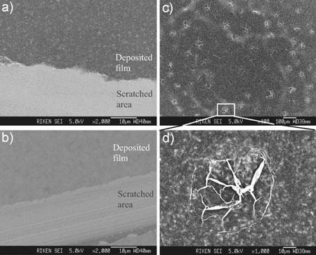
| Morphology and deposition conditions. a–d) FE-SEM images of deposited samples. (a and b have scratched areas, for focusing purposes). Sample a) magnification: 2000x; b) magnification: 2000x; c) magnification: 100x; d) enlarged image of c, magnification: 1000x (Reprinted with permission from Wiley-VCH Verlag) | |
| Previous attempts to use the electrospray-deposition technique for OLED fabrication have failed to produce polymer films that compete with other fabrication techniques. The RIKEN researchers decided to use a combination of two solvents to improve this technique, which uses a thin glass capillary with the polymer solution stored inside and a conductive wire inserted in it. When a high voltage is applied between this conductive wire and the OLED electrodes on the substrate, the solution sprays out of the capillary end as atomized droplets that are attracted to the substrate by electrostatic force. This means there is little solution wastage as the spray is highly directed. | |
| In morphology tests, Yamagata and his team discovered that three different deposition modes – particle, wet, and thin film – occur depending on the solvent mixture ratio and sample concentration. They also found that the first solvent evaporated rapidly after the atomization of the solution, leaving a small amount of the second solvent, which has a higher boiling point, in the droplets. When the polymer concentrations were finely tuned, the carefully chosen second solvent enabled the not-quite-dry atomized droplets to form a smooth, continuous film of high quality over the OLED electrode. Because the films dry quickly on the surface, it should be easy to fabricate multilayer devices without mixing of materials between layers. | |
| From a series of comparative experiments, the researchers found that devices fabricated from electrospray-deposited films turned on at lower voltages and could support higher current densities than ones made from spin-coated films. At low voltages, the electrospray deposition also enabled higher pixel intensity. | |
| “We have discovered a range of conditions using a two-solvent method that can make extremely smooth thin films using electrospray deposition,” says Yamagata. “Using this technology these devices could be manufactured as inexpensively as printing newspapers.” | |
| So far, the RIKEN team has focused on film deposition morphology in various conditions, but they say that in the future more detailed analysis of the characteristics of OLED materials, such as the luminescence spectrum, quantum efficiency and the multilayered structure, should be tested. | |
 By
Michael
Berger
– Michael is author of three books by the Royal Society of Chemistry:
Nano-Society: Pushing the Boundaries of Technology,
Nanotechnology: The Future is Tiny, and
Nanoengineering: The Skills and Tools Making Technology Invisible
Copyright ©
Nanowerk LLC
By
Michael
Berger
– Michael is author of three books by the Royal Society of Chemistry:
Nano-Society: Pushing the Boundaries of Technology,
Nanotechnology: The Future is Tiny, and
Nanoengineering: The Skills and Tools Making Technology Invisible
Copyright ©
Nanowerk LLC
|
|
|
Become a Spotlight guest author! Join our large and growing group of guest contributors. Have you just published a scientific paper or have other exciting developments to share with the nanotechnology community? Here is how to publish on nanowerk.com. |
|