| Posted: Nov 24, 2009 | |
Photonic-plasmonic device fully compatible with AFM and Raman spectroscopy |
|
| (Nanowerk Spotlight) Single molecule detection requires tools that have the detection sensitivity at the scale of single molecules. This could mean a spatial resolution requirement of only a few nanometers especially if the precise location of the molecule needs to be mapped. Researchers have already developed spectroscopic techniques capable of physical and chemical mapping on a nanometer scale. Researchers in Italy have now reported the design, fabrication and application of a photonic–plasmonic device that is fully compatible with atomic force microscopy and Raman spectroscopy – an approach that is novel in both scientific and technological aspects. | |
| "In fact, we not only designed a hybrid device on an atomic force microscope (AFM) cantilever that combines photonic crystal and plasmonic waveguides, but we also fabricated an almost ideal cone-shaped waveguide that allows a controlled tri-dimensional generation of plasmonic compression of the electromagnetic field in the apex of the cone," Enzo di Fabrizio explains to Nanowerk. "Without this progress in fabrication technology these tools would remain interesting only theoretically." | |
| Di Fabrizio is Director of the nanofabrication department at IIT (Italian Institute of Technology) in Genoa, and full professor in the department of medicine at the Universití della Magna Graecia in Catanzaro, Italy, as well as the Chief Scientist of the university's BIONEM laboratory. | |
| Reporting their findings in the November 22, 2009 online issue of Nature Nanotechnology ("Nanoscale chemical mapping using three-dimensional adiabatic compression of surface plasmon polaritons), the team describes the fabrication and demonstrates the first application of a device that, by combining different photonic concepts, materials and architectures, allows the generation of strongly localized surface plasmon polaritons (SPPs) to obtain a chemical map at the same spatial resolution of an AFM. | |
| The paper is an interdisciplinary effort by five Italian institutions: IIT (Italian Institute on Technology (Italian twin institute of MIT), University of Pavia, department of Physics, University of Magna Graecia, Catanzaro, TASC and CBM laboratories of Trieste. | |
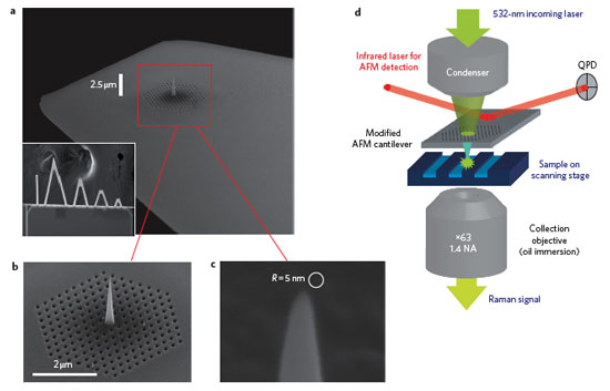
| The device consists of a two-dimensional dielectric photonic crystal cavity patterned on an AFM cantilever, together with a tapered silver waveguide placed at the center of the cavity. The waveguide is a 2.5 µm-tall metallic cone. The entire device is fabricated by means of ion milling and electron-beam induced deposition and can be fully integrated with an inverted Raman microscope combined with an AFM stage. | |
 |
|
| Tapered waveguide on an AFM cantilever and experimental apparatus. a, Scanning electron microscope image of the device fabricated on a set of silicon nitride AFM cantilevers. The inset shows the whole chip with multiple tips. b,c, Close-up images of the photonic crystal cavity, fabricated on the silicon nitride membrane, and the tapered plasmonic waveguide with a conical shape and radius of curvature at the apex of 5 nm. d, Sketch of the experimental setup, showing the integration of the photonic–plasmonic device into an AFM–Raman microscope. The nanofabricated AFM tips and silicon nanocrystal sample are mounted on the AFM tip holder and on the sample stage, respectively (Nanowizard II, JPK Berlin). The AFM is equipped with a special module (TAO, JPK Berlin) that allows independent scanning of the tip or the sample in an area of 100x100 µm2, with a scanning step resolution better than 1 nm. The sample and AFM tip can therefore be aligned independently with respect one another and the optical axis of the microscope. AFM cantilever deflection is monitored through a conventional laser beam deflection system with an infrared laser (λ=860 nm) and detected by a four-quadrant photodiode (QPD). Raman and AFM laser spectral regions are separated and do not overlap. (Reprinted with permission from Nature Publishing Group) | |
| "With our home-built Raman AFM we combined the three techniques of optical microscopy, Raman spectroscopy and AFM," says di Fabrizio. "In this way we were able to simultaneously obtain a chemical map at 5-7 nm spatial resolution." | |
| In order to achieve such a result, the team exploited and generated surface plasmon polaritons through a physical mechanism called adiabatic compression, proposed theoretically by Mark Stockman from Georgia State University in 2004 ("Nanofocusing of Optical Energy in Tapered Plasmonic Waveguides). This mechanism is responsible of the concentration of electromagnetic energy in a region limited just around the apex of a cone-like wave guide. This region is approximately comparable to the radius of curvature of the cone apex. The best results achieved by the Italian team was a 2.5 nm radius of curvature. | |
| Di Fabrizio points out that the development of a photonic–plasmonic device that is fully compatible with AFM and Raman spectroscopy opens up a number of significant opportunities in the nanoscale chemical mapping of materials. | |
| "The approach could be of particular benefit in the nanoscale analysis of biological matter," he says. "We believe that device architectures based on the adiabatic generation of SPPs have considerable potential for applications in which a reliable nanometer-sized light source is of utmost importance." | |
| Di Fabrizio and co-authors are already aiming at applying the idea to mapping biological molecules in in vivo conditions. "We are already working on membrane proteins and trying to combine the Raman signature with spatial resolution and with force spectroscopy through an AFM microscope," he says. "This combination will provide new information on the structural conformation of a living protein directly on a living cell without using crystallization, or in particular, with protein that can not be crystallized. Moreover this approach should allow to see mutation in the protein even at level of single amino acid substitution, especially for small peptides." | |
| "It is our dream to apply this results also to time-resolved spectroscopy. This means the possibility to get information on reactions or conformational dynamical changes, even for biological molecules. This will help in understanding the functional behavior of proteins." | |
 By
Michael
Berger
– Michael is author of three books by the Royal Society of Chemistry:
Nano-Society: Pushing the Boundaries of Technology,
Nanotechnology: The Future is Tiny, and
Nanoengineering: The Skills and Tools Making Technology Invisible
Copyright ©
Nanowerk LLC
By
Michael
Berger
– Michael is author of three books by the Royal Society of Chemistry:
Nano-Society: Pushing the Boundaries of Technology,
Nanotechnology: The Future is Tiny, and
Nanoengineering: The Skills and Tools Making Technology Invisible
Copyright ©
Nanowerk LLC
|
|
|
Become a Spotlight guest author! Join our large and growing group of guest contributors. Have you just published a scientific paper or have other exciting developments to share with the nanotechnology community? Here is how to publish on nanowerk.com. |
|