| Posted: Dec 02, 2009 | |
Graphene nanotechnology for tomorrow's nanoelectronic circuits |
|
| (Nanowerk Spotlight) The success of the computer and communications industry is mainly due to the possibility of a large volume and low cost production output: silicon wafers containing myriad micro and nano structures are at the basis of Complementary Metal Oxide Semiconductor (CMOS) technology. Chip structures already have reached nanoscale dimensions but as they continue to shrink below the 20 nanometer mark, ever more complex challenges arise and scaling appears not to be economically feasible any more. And below 10 nm, the fundamental physical limits of CMOS technology will be reached. | |
| One promising material that could enable the chip industry to move beyond the current CMOS technology is graphene, a monolayer sheet of carbon. Numerous nanotechnology labs and consortia, like the European GRAND (Graphene-based Nanoelectronic Devices) are exploring graphene-based nanoelectronics. Notwithstanding the intense research interest, large scale production of single layer graphene remains a significant challenge. | |
| Researchers at Cornell University have now reported a new technique for producing large scale (>1 cm) single layer graphene sheets and fabricating transistor arrays with uniform electrical properties directly on the device substrate. | |
 |
|
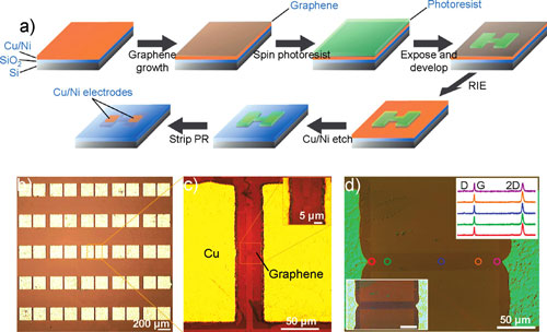
| Fabrication of single layer graphene device array. (a) Schematic of device fabrication procedure (see main text for details). (b) Brightfield optical image of a typical sample substrate after fabrication. (c) Close-up brightfield image of the same sample. Graphene connecting the copper pad is just visible (boxed). Inset: Image of the device channel (100x, NA = 0.9). (d) Differential interference contrast image of a longer device. Upper inset: Raman spectra across the length of the graphene strip are highly uniform. Lower inset: brightfield image of the sample. All brightfield images have been contrast enhanced. (Reprinted with permission from American Chemical Society) | |
| "Our new single layer graphene synthesis and device fabrication method is compatible with standard thin film technologies and does not involve any nonconventional and delicate steps such as liquid based transfer" says Jiwoong Park, an assistant professor at Cornell's Department of Chemistry and Chemical Biology. "Thus, it can allow single layer graphene to be integrated into large scale electronics circuitry with only minor steps that can easily be streamlined and automated." | |
| Full integration of graphene into conventional chip circuits requires a reproducible and scalable technique for large-scale graphene synthesis that is compatible with conventional thin film technology. | |
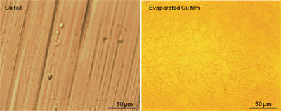
| Park's group uses copper to grow their single layer graphene. Although the basic mechanism is similar to the one reported earlier this year ("Large-Area Synthesis of High-Quality and Uniform Graphene Films on Copper Foils"), the Cornell team uses an evaporated copper film instead of a copper foil. | |
 |
|
| Side by side comparison of growths on a copper foil (left) and an evaporated copper thin film (right). Feature sizes appear to be much larger for copper foils than for copper thin films. (Reprinted with permission from American Chemical Society) | |
| Park says that this is a significant technological improvement and allows them to directly fabricate uniform transistor arrays without a transfer process. This finding leads to a low device failure rate (<5%) and uniform electrical properties. Also, the technique is limited only by the size of the substrate and growth chamber. | |
| The growth substrate is a copper film of varying thickness with a thin nickel adhesion layer, both directly evaporated onto a silicon wafer covered with a thermal oxide. The researchers found that one of the key variables for the quality of the graphene is the thickness of the copper film. | |
| This method allows the fabrication of a large scale device array with a simple photolithography process. One key advantage of this process is its high yield and uniform electrical properties. In order to show this, Park's team fabricated 95 devices on a single substrate over a large area (approx. 3-6 mm) with varying channel length and width. They achieved a 97% success rate. | |
| Park says that he anticipates that additional synthesis optimization and materials characterization will further improve already promising electrical and physical characteristics of large scale single layer graphene. | |
| The team has reported their findings in the October 27, 2009 online edition of Nano Letters ("Transfer-Free Batch Fabrication of Single Layer Graphene Transistors"). | |
 By
Michael
Berger
– Michael is author of three books by the Royal Society of Chemistry:
Nano-Society: Pushing the Boundaries of Technology,
Nanotechnology: The Future is Tiny, and
Nanoengineering: The Skills and Tools Making Technology Invisible
Copyright ©
Nanowerk LLC
By
Michael
Berger
– Michael is author of three books by the Royal Society of Chemistry:
Nano-Society: Pushing the Boundaries of Technology,
Nanotechnology: The Future is Tiny, and
Nanoengineering: The Skills and Tools Making Technology Invisible
Copyright ©
Nanowerk LLC
|
|
|
Become a Spotlight guest author! Join our large and growing group of guest contributors. Have you just published a scientific paper or have other exciting developments to share with the nanotechnology community? Here is how to publish on nanowerk.com. |
|