| Posted: Dec 07, 2009 | |
Curvilinear electronics that fit golf balls and body parts |
|
| (Nanowerk Spotlight) As we showed you in previous Nanowerk Spotlights, the future of electronics will be very different from the planar and brittle semiconductor chips we are used to today. Future electronic circuits will be on anything you can think of – and probably most interesting on things you can't even think of today (see for instance: "Nanotechnology electronics at the tip of your gloved finger "). | |
| The key for most visionary electronic applications will be printability, i.e. that the circuits can be applied to any material, and flexibility, i.e. that they can adhere to any shape or form – even body parts. Imagine an ultrathin film of electronic circuits attached to internal organs like your heart to monitor vital functions. | |
| "All existing forms of electronics are built on the two-dimensional, planar surfaces of either semiconductor wafers or plates of glass," John Rogers explains to Nanowerk. "Mechanically flexible circuits based on organic semiconductors are beginning to emerge into commercial applications, but they can only be wrapped onto the surfaces of cones or cylinders – they cannot conform to spheres or any other type of surface that exhibits non-Gaussian curvature. Applications that demand conformal integration, e.g. structural or personal health monitors, advanced surgical devices, or systems that use ergonomic or bio-inspired layouts, etc., require circuit technologies in curvilinear layouts." | |
 |
|
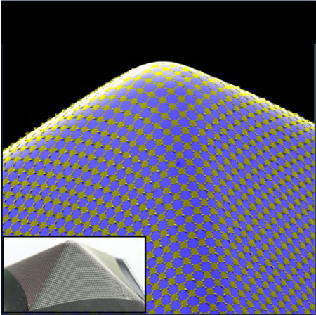
| Silicon circuit mesh wrapped onto a pyramidal substrate. (Image: Rogers Group, University of Illinois) | |
| Rogers' research at the University of Illinois is geared to address that challenge, preferably by using well developed, high performance semiconductors like silicon. We have covered several of his group's recent developments here in our Spotlight series. See for instance "Gutenberg + nanotechnology = printable electronics " about printable electronics or "One molecule thick nanotechnology membranes take shape " about monolayer membranes. | |
| In his most recent work, Rogers and his group, together with collaborators from Northwestern University, Korea University and Tsinghua University, have discovered that it is possible to wrap silicon electronics around objects with arbitrary curvilinear shapes – something that is impossible with wafer-based technologies. The strategy combines circuits in optimized, mesh layouts with elastomeric transfer elements that accomplish the wrapping process. | |
| "The use of purely elastic mechanics together with hybrid plastic/inorganic circuit meshes enables predictive analysis and high strain deformations, respectively," says Rogers. "These aspects represent important distinguishing features compared to similar work performed by other groups." | |
| Reporting their findings in a recent issue of Small ("Curvilinear Electronics Formed Using Silicon Membrane Circuits and Elastomeric Transfer Elements") the team reports advanced concepts for conformal wrapping of silicon-based circuits, initially fabricated in 2D layouts with standard or moderately adapted forms of conventional techniques, onto surfaces with a range of curvilinear shapes. | |
| Rogers explains that his team's strategy uses structured silicon membranes with thin polymer/metal interconnects, in non-coplanar mesh layouts. "The result embodies combined aspects of concepts recently reported for electronic eye cameras and for stretchable electronics to achieve new and general capabilities for curvilinear electronics on surfaces with nearly arbitrary shapes." | |
  |
|
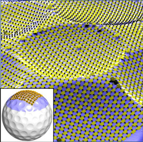
| Left: Silicon circuit mesh on the surface of a golf ball. Right: An individual circuit. (Images: Rogers Group, University of Illinois) | |
| The process begins with fabrication of a thin transfer element in an elastomer such as PDMS by double-casting and thermal-curing against the object to be wrapped (i.e., the target substrate like the golf ball in the image above). Radially stretching the resulting element from its rim forms a flat drumhead membrane in which all points in the PDMS are in tension with levels of strain that vary with position. | |
| Contacting this stretched transfer element against a prefabricated circuit in a planar, ultrathin mesh geometry on a silicon wafer and then peeling it backlifts the circuit on to the PDMS. Relaxing the tension geometrically transforms the membrane and the circuit on its surface into the shape of the target substrate. During this process, the interconnection bridges of the mesh adopt non-coplanar arc shapes, thereby accommodating the compressive forces in a way that avoids significant strains in the islands. Transfer to the corresponding region of the target substrate and removal of the rim completes the process. | |
| Rogers says that his group is already deep into the development of completely new classes of biomedical devices that provide intimate integration between high functionality electronics and sensors and the human body. These approaches in these cases – as yet unpublished – represent extensions of the ideas outlined above. | |
 By
Michael
Berger
– Michael is author of three books by the Royal Society of Chemistry:
Nano-Society: Pushing the Boundaries of Technology,
Nanotechnology: The Future is Tiny, and
Nanoengineering: The Skills and Tools Making Technology Invisible
Copyright ©
Nanowerk LLC
By
Michael
Berger
– Michael is author of three books by the Royal Society of Chemistry:
Nano-Society: Pushing the Boundaries of Technology,
Nanotechnology: The Future is Tiny, and
Nanoengineering: The Skills and Tools Making Technology Invisible
Copyright ©
Nanowerk LLC
|
|
|
Become a Spotlight guest author! Join our large and growing group of guest contributors. Have you just published a scientific paper or have other exciting developments to share with the nanotechnology community? Here is how to publish on nanowerk.com. |
|