| Posted: Dec 09, 2009 | |
Free-standing nanosieve membranes that are only 1 nanometer thick |
|
| (Nanowerk Spotlight) Ultrathin nanosieves with a thickness smaller than the size of the pores are especially advantageous for applications in materials separation since they result in an increase of flow across the nanosieve. Separation of complex biological fluids can particularly benefit from novel, chemically functionalized nanosieves, since many bioanalytical problems in proteomics or medical diagnostics cannot be solved with conventional separation technologies. | |
| Researchers in Germany have now fabricated chemically functionalized nanosieves with a thickness of only ∼1 nm – the thinnest free-standing nanosieve membranes that have been reported so far. | |
| "We have shown a novel path to the fabrication of large area (up to 1 square millimeter), chemically functionalized nanosieves with a thickness of only about 1 nm," Andrey Turchanin tells Nanowerk. "This path is based on the utilization of self-assembled monolayers and their modification with EUV interference lithography (EUV-IL) or electron beam lithography (EBL)." | |
| Turchanin, a researcher at the faculty of physics at Bielefeld University, explains that the size of the nanoholes in the membranes can be flexibly adjusted down to 30 nm by choosing appropriate conditions for lithography. He also points out that electron-beam lithography or other exposure methods may be used instead of the EUV-IL that the team utilized. | |
| "As both faces of the membranes are chemically distinct by amino and thiol/dissulfide groups, respectively, this opens possibilities for further functionalization," he explains. "The nanosieves can be used as templates for deposition of metal to form composite nanosieves." | |
 |
|
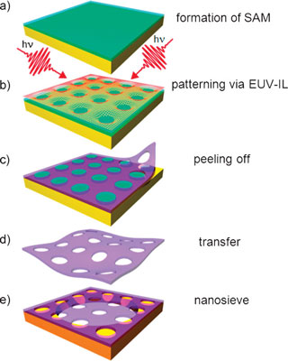
| Fabrication scheme of nanosieve membranes. a) A SAM of NBPT is formed on a gold substrate. b) Generation of amino-terminated crosslinked areas (nanosheets) in theSAMvia EUV-IL. c) Spin-coating of a polymer film and peeling off from the gold substrate. d) Transfer of the nanosheet with the hardened polymer. e) Formation of a 1-nm-thin freestanding nanosieve by dissolving the polymer on a new holey substrate. (Reprinted with permission from Wiley-VCH Verlag) | |
| To fabricate the nanosieves, the researchers worked with self-assembled monolayers (SAMs) of aromatic thiols on a gold substrate. They then generated a perforated amino-terminated nanosheet in the thiol group SAM by EUV-IL, peeled it off and, in a last step, transferred it on a new holey substrate, which results in a 1-nm-thin nanosieve. | |
| "In order to transfer the perforated nanosheet onto a new substrate, we spin-coated a polymer film (PMMA) onto the sample surface," says Turchanin. "Immersion of the sample into the etching solutions results in the release of the polymer film with adhered crosslinked areas from the gold substrate, while the non-crosslinked regions dissolve in the etchants." | |
| The perforated nanosheet is stabilized by the hardened polymer film and can be simply transferred to a variety of other materials, such as flat silicon substrates. After such a transfer, the polymer is dissolved by dipping the sample into the solvent and the perforated nanosheet of the crosslinked amino-terminated SAM is left on a new surface. | |
| The resulting nanosieves have regular arrays of nanopores with a diameter of down to 30 nm and possess a distinct chemical functionality on each side. That makes them some kind of 'Janus membrane' with two chemically different sides, which allows for further specific chemical functionalization with e.g. biocompatible materials. | |
| According to Turchanin, the main future challenge now is the implementation of the nanosieves in microfluidic systems and tests of their functionality in bioseparation applications. | |
| The researchers reported their findings in a recent issue of Small ("Chemically Functionalized Carbon Nanosieves with 1-nm Thickness"). | |
 By
Michael
Berger
– Michael is author of three books by the Royal Society of Chemistry:
Nano-Society: Pushing the Boundaries of Technology,
Nanotechnology: The Future is Tiny, and
Nanoengineering: The Skills and Tools Making Technology Invisible
Copyright ©
Nanowerk LLC
By
Michael
Berger
– Michael is author of three books by the Royal Society of Chemistry:
Nano-Society: Pushing the Boundaries of Technology,
Nanotechnology: The Future is Tiny, and
Nanoengineering: The Skills and Tools Making Technology Invisible
Copyright ©
Nanowerk LLC
|
|
|
Become a Spotlight guest author! Join our large and growing group of guest contributors. Have you just published a scientific paper or have other exciting developments to share with the nanotechnology community? Here is how to publish on nanowerk.com. |
|