| Posted: Dec 14, 2009 | |
New imaging technique allows quick evaluation of graphene sheets |
|
| (Nanowerk Spotlight) Graphene based sheets such as pristine graphene, graphene oxide, or reduced graphene oxide – also known as chemically modified graphene – are basically single atomic layers of carbon network. They are the world's thinnest materials. A general visualization method that allows quick observation of these sheets would be highly desirable as it can greatly facilitate sample evaluation and manipulation, and provide immediate feedback to improve synthesis and processing strategies. | |
| Current imaging techniques for observing graphene based sheets include atomic force microscopy, transmission electron microscopy, scanning electron microscopy and optical microscopy. Some of these techniques are rather low-throughput. And all the current techniques require the use of special types of substrates. This greatly limits the capability to study these materials. | |
| For example, graphene based sheets have been used for making flexible, transparent electronic devices on plastic substrate. However, it has been quite challenging to visualize these materials on plastic substrates. Moreover, solution processing of graphene based materials is most promising for scaling up the production. However, no current technique has been demonstrated to be capable of seeing these sheets in solution, which would otherwise help researchers to understand their solution dynamics. | |
| Researchers from Northwestern University have now reported a new method, namely fluorescence quenching microscopy (FQM), for visualizing graphene-based sheets. The contrast mechanism is based on fluorescence quenching, thus eliminating the need for special types of substrates. This allows high-throughput, high-contrast imaging of on graphene-based sheets on arbitrary substrates and even in solution, which have been very difficult, if not impossible tasks using current microscopy techniques. | |
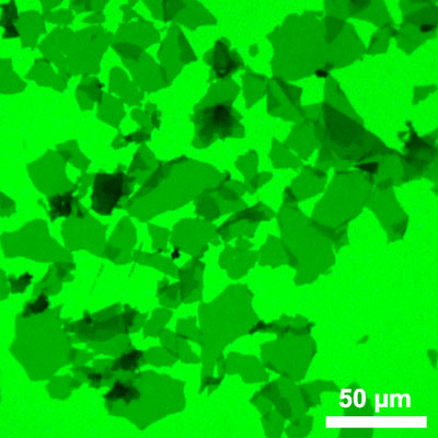
| "It has been well-known that graphitic systems such as carbon nanotubes can strongly quench the emission of nearby dye molecules" says Jiaxing Huang, an assistant professor at Northwestern's Department of Materials Science & Engineering. "In fact, it makes fluorescent labeling of graphene based sheets very inefficient. Now, in a reverse strategy, we simply spin-coat a dye/polymer layer on the graphene based sheets, which upon excitation reveals the underlying graphene materials as dark sheets in a bright background as illustrated in the figure below." | |
 |
|
| Visualizing graphene based single atomic layers by fluorescence quenching microscopy (FQM). (Image: Jiaxing Huang, Northwestern University) | |
| Reporting their findings in the December 4, 2009 online issue of JACS ("Visualizing Graphene Based Sheets by Fluorescence Quenching Microscopy"), Huang and his team demonstrate that FQM images can offer comparable layer resolution to AFM and SEM. | |
| "In fact" says Huang, "when we made the above image in gray scale, people often times thought it was a SEM image!" | |
| The FQM method lifts the need for special substrates (e.g., conducting, atomically smooth, or dielectric-coated silicon, etc) and works with a wide range of fluorescent materials and polymers including resist materials used in photolithography and e-beam lithography. It therefore should enable high-throughput imaging in many applications. Of particular interests are the new capabilities to visualize graphene based sheets on plastic surface and in solution. Huang says that researchers now can easily study how solution-processing techniques affect the thin-film microstructure for graphene based plastic electronic devices. | |
| "FQM allows high-throughput sample evaluation to improve graphene synthesis, or to check the quality of graphene films deposited on plastics substrates," explains Huang. "In our own lab, we have now used FQM to replace SEM and AFM for most of our imaging needs." | |
| Going forward, the Northwestern team plans to apply this for high-throughput sample evaluation to improve the synthesis and processing of graphene based sheets and to integrate FQM with photolithography. They would also like to conduct more investigations of the fluorescence quenching mechanism by graphene based sheets. | |
 By
Michael
Berger
– Michael is author of three books by the Royal Society of Chemistry:
Nano-Society: Pushing the Boundaries of Technology,
Nanotechnology: The Future is Tiny, and
Nanoengineering: The Skills and Tools Making Technology Invisible
Copyright ©
Nanowerk LLC
By
Michael
Berger
– Michael is author of three books by the Royal Society of Chemistry:
Nano-Society: Pushing the Boundaries of Technology,
Nanotechnology: The Future is Tiny, and
Nanoengineering: The Skills and Tools Making Technology Invisible
Copyright ©
Nanowerk LLC
|
|
|
Become a Spotlight guest author! Join our large and growing group of guest contributors. Have you just published a scientific paper or have other exciting developments to share with the nanotechnology community? Here is how to publish on nanowerk.com. |
|