| Posted: Dec 29, 2006 | |
Blow-up: The startling landscapes of nanotechnology |
|
| (Nanowerk Spotlight) The nanoworld cannot be portrayed with a camera, nor can it be seen even with the most powerful optical microscope. Only special instruments have access to images of the nanoworld. A fascinating new exhibition "Blow-up: images from the nanoworld" in Modena/Italy shows the work of scientists associated with the National Center on Nanostructures and Biosystems at Surfaces in Modena, Italy, headed by Elisa Molinari. | |
| The images have been manipulated in a variety of ways by photographer, Lucia Covi. Covi is particularly sensible to the aesthetic paradigms of scientists: her gaze thus grasps essential aspects of the portrayed objects and allows her to shine them with a new light, as they are revealed now. This exhibition brings to the public images that are usually accessible to few, because they remain confined in the research laboratories, on the scientists' desks. | |
| The images are stills that, over time, have been put together from different framings, and that we can look at thanks to the mediation of machines. Some of them represent exceptional events, outstanding results that ended on the cover of scientific journals. Others were born from everyday research. All of them show a landscape that is being unraveled by scientists, scenery that is very different from the one we can see in the media, largely obtained through computer graphics and "artistic" interpretations, when not directly borrowed from science fiction. | |
 |
|
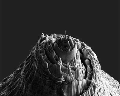
| Scanning near-field optical microscopy (SNOM) uses nanoscale metal tips to scan a surface. Here, a standard tip has been modified and sharpened to increase its precision. The tip in the middle of this structure measures a few tens of nanometers. (Image: G.C. Gazzadi, S3 (INFM-CNR), Modena; P.Gucciardi, CNR-IPCF, Messina. Artwork: Lucia Covi) | |
 |
|
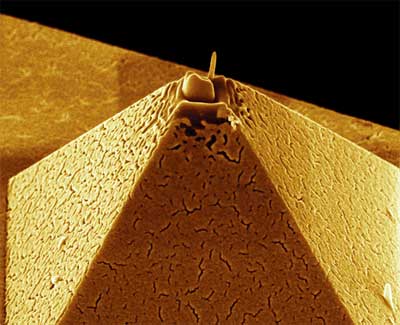
| Developing new instruments to be able to "see" at the nanoscale is a research field in itself. Shown here is the tip of an atomic force microscope (AFM), one of the foremost tools for imaging, measuring and manipulating matter at the nanoscale. Here, a platinum electrode measuring one hundredth of a nanometer has been deposited on the tip of this pyramid shaped AFM tip via focused ion beam (FIB) deposition. (Image: C. Menozzi, G.C. Gazzadi, S3 (INFM-CNR), Modena. Artwork: Lucia Covi) | |
 |
|
| Top view of a hole carved in a polyethylene surface. During a series of experiments the use of a FIB has proven to be very versatile and capable of carving various materials, including plastic. (Image: G.C. Gazzadi, S3 (INFM-CNR), Modena. Artwork: Lucia Covi) | |
 |
|
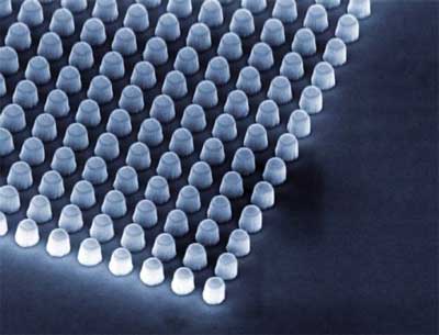
| Scanning electron microscope (SEM) image of quantum dots fabricated through electron beam lithography and subsequent dry-chemical etching on a quasi bidimensional layer (GaAl heterostructure). These structures are used to study the behavior of electrons, which are confined into tiny spaces – approximate. 10 electrons per dot. The diameter of each quantum dot is 200 nm (which means that a billion of these structure easily fit on the tip of your finger). (Image: C.P. Garcia, V. Pellegrini , NEST (INFM), Pisa. Artwork: Lucia Covi) | |
 |
|
| SEM image of a micron sized trench (10 x 20 x14 µm3) in a Cu/SiO2/Si multilayer, obtained through FIB milling. The precision of this technique allows the visualization of ultrathin (tens of nanometers) layers. (Image: G.C.Gazzadi, S.Frabboni, S3 (INFM-CNR), Modena. Artwork: Lucia Covi) | |
 |
|
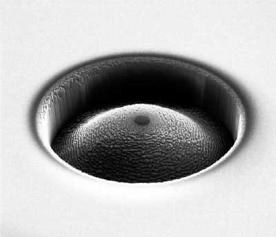
| SEM image of a work sample on a magnesium oxide surface using FIB. The diameter of the hole measures approximate. 4 µm. (Image: G.C. Gazzadi, A. Spessot, S3 (INFM-CNR), Modena. Artwork: Lucia Covi) | |
 |
|
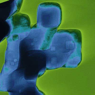
| Tiny spaces have formed inside titanium dioxide nanocrystals, as shown in this SEM image. The square structure of these inside spaces, which measure between 20 nm and 40 nm, is due to the crystalline structure of the material. (Image: L. Nasi, IMEM (CNR), Parma. Artwork: Lucia Covi) | |
 By
Michael
Berger
– Michael is author of three books by the Royal Society of Chemistry:
Nano-Society: Pushing the Boundaries of Technology,
Nanotechnology: The Future is Tiny, and
Nanoengineering: The Skills and Tools Making Technology Invisible
Copyright ©
Nanowerk LLC
By
Michael
Berger
– Michael is author of three books by the Royal Society of Chemistry:
Nano-Society: Pushing the Boundaries of Technology,
Nanotechnology: The Future is Tiny, and
Nanoengineering: The Skills and Tools Making Technology Invisible
Copyright ©
Nanowerk LLC
|
|
|
Become a Spotlight guest author! Join our large and growing group of guest contributors. Have you just published a scientific paper or have other exciting developments to share with the nanotechnology community? Here is how to publish on nanowerk.com. |
|