| Posted: Feb 24, 2010 | |
Borrowing from nature's nanofabrication tricks - biomimetic crystallization nanolithography |
|
| (Nanowerk Spotlight) Numerous research groups around the world are inspired by the biomineralization processes found in nature – the process by which living organisms produce inorganic materials (minerals) found in bones, teeth, or shells. In this process, the formation of the mineral is controlled with great precision by specialized organic biomolecules such as sugars and proteins. Whereas the fabrication of many man-made crystals requires elevated temperatures and strong chemical solutions, nature's organisms have long been able to lay down elaborate mineral structures at ambient temperatures. Being able to duplicate nature's 'production process' would potentially allow for much simpler and 'greener' fabrication technologies than the ones employed today (see: "Peacock feathers and butterfly wings inspire bio-templated nanotechnology materials"). | |
| "Despite the great success of this bioinspired approach, it would be desirable to find a methodology to pattern these biomimetically synthesized materials in desired shapes and dimensions for their integration in electronic components of complex circuits and microprocessors, energy-storage systems, solar cells, optics, and sensors," Hiroshi Matsui tells Nanowerk. "To that end, we have developed a new nanofabrication methodology to generate crystalline oxide semiconductor nanopatterns under mild conditions." | |
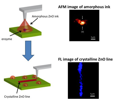
| This new technique – Biomimetic Crystallization Nanolithography (BCN) – developed by Matsui and his team at Hunter College in New York, is a new type of scanning probe nanolithography that allows the patterning of highly crystalline oxide semiconductor by writing amorphous inks and inducing the crystallization of these material simultaneously due to the patterning process. | |
 |
|
| Schematic of biomimetic crystallization nanolithography. (Images: Dr. Matsui, City University of New York–Hunter College ) | |
| While previous bio-inspired approaches were able to synthesize crystalline oxide semiconductors such as zinc oxide in mild conditions and at room temperature, patterning highly crystalline semiconductors at the nanoscale needs sophisticated techniques. | |
| "BCN has the advantage of patterning the material in desired shapes in the simple manner and the integration with the circuitry is straightforward, useful for nano optic and nanoelectronic applications" explains Matsui. "By tuning the parameters of the lithography step it is possible to control the size and shape of the as-generated nanocrystals in the pattern." | |
| In other scanning nanolithography approaches such as dip-pen nanolithography (DPN) the AFM tip is used as a mere pen to write chemical inks. In BCN the tip also induces a physicochemical change in the ink to generate crystalline semiconducting nanopatterns. The combination of these two functions (patterning + crystallization) in a single step is the novelty of BCN. | |
| Reporting their findings in the January 19, 2010 online issue of Angewandte Chemie International Edition ("Biomimetic Crystallization Nanolithography: Simultaneous Nanopatterning and Crystallization"), Matsui and his team show that by carefully selecting the parameters of the lithography step such as tip velocity, the kinetics of crystal growth can also be controlled to yield oxide semiconductor nanocrystals in reproducible morphology and dimensions. | |
| Matsui explains how the process works: "To draw crystalline zinc oxide nanowires on silicon at room temperature by BCN, highly hydrated amorphous intermediates are required as inkwells for the writing on the substrate, and these amorphous inks are produced by the enzyme urease, which becomes the nucleation point for the reaction. After addition of the enzyme substrate urea, the urease on the silicon substrate produces ammonia, and the resulting increase in pH value provides the necessary hydroxy groups for the growth of the oxide around the enzyme." | |
| BCN will allow to write small features of oxide semiconductor at desired positions. For example, two desired electrodes can be interconnected by semiconductor nanowires without lithography. | |
| Matsui points out that, since BCN can generate semiconducting nanopatterns at desired locations on a substrate, it has a myriad of potential applications such as in the fabrication of electronic nanodevices, nanosensors or in nano optics because the integration with the other elements of the circuit is straightforward. | |
| "The density of nanocrystals in a pattern could be tuned to be continuous by reducing the viscosity of the ink by varying the water content and polymerization degree of the amorphous intermediate" says Matsui. "The inkwells can be generated at designated locations on the substrate by patterning urease with established electrostatic protein placement and DPN techniques, before triggering the mineralization process so that one can have more freedom to design further complex nanowire patterns by BCN." | |
| While the team found the ideal condition for patterning zinc oxide, they caution that it may take time to find amorphous inks for other semiconductor materials. | |
 By
Michael
Berger
– Michael is author of three books by the Royal Society of Chemistry:
Nano-Society: Pushing the Boundaries of Technology,
Nanotechnology: The Future is Tiny, and
Nanoengineering: The Skills and Tools Making Technology Invisible
Copyright ©
Nanowerk LLC
By
Michael
Berger
– Michael is author of three books by the Royal Society of Chemistry:
Nano-Society: Pushing the Boundaries of Technology,
Nanotechnology: The Future is Tiny, and
Nanoengineering: The Skills and Tools Making Technology Invisible
Copyright ©
Nanowerk LLC
|
|
|
Become a Spotlight guest author! Join our large and growing group of guest contributors. Have you just published a scientific paper or have other exciting developments to share with the nanotechnology community? Here is how to publish on nanowerk.com. |
|