| Posted: Mar 02, 2010 | |
Investigating solar cells with AFM and confocal microscopy |
|
| (Nanowerk Spotlight - Application Note) Solar cells, or photovoltaic cells, are used to convert sunlight into electrical power. As traditional power sources grow scarce, other forms of producing electrical power are gaining firm footing in the power supply mix. Solar cells are already widely used in a variety of applications - from spacecraft, to small portable devices, to farm installations, to roadway signs. As energy prices increase, public demand for solar power has surged. In order to meet the longevity, yield, and price requirements of consumers and industry, public and private sector research has increased dramatically. | |
| While traditional tools are helpful to investigate and improve solar cells, AFM/SPM offers metrology, topography & roughness analysis at much higher resolution than with optical techniques. In addition AFM/SPM techniques can be used to measure electronic properties of samples, such as work function. | |
 |
|
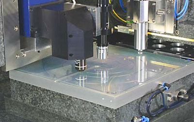
| Close up of the N8 TITANOS sample stage, showing the confocal microscope, a video microscope and NANOS (AFM/SPM scanning head). The sample stage accommodates samples up to 300 mm x 300 mm. Every position on the sample is available for rapid inspection. | |
| Technical details | |
| All measurements were performed on an N8 TITANOS built for the FZ Jülich, Institute for Energy Research (Photovoltaics), and modified slightly to include a highperformance confocal microscope instead of the standard optical microscope. The N8 TITANOS is a high-resolution, large sample AFM that can measure with atomic-scale resolution anywhere on a 300 mm wafer, with precise repositioning under two or more measurement stations (AFM, confocal microscope etc). | |
 |
|
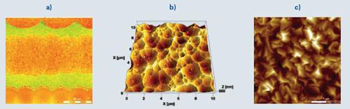
| Measurements on solar cell components: a) Confocal microscope image of a thin film solar cell, image size: 158 µm x 158 µm, Z-height: 6 µm; b) Intermittent contact mode AFM scan of ZnO, image size: 10 µm x 10 µm, Z-height: 673 nm; c) Contact mode AFM scan of SnO2, image size: 3 µm x 3 µm, Z-height: 229 nm | |
| The thin film solar cells were kindly supplied by the FZ Jülich, IER. Research into the Transparent Conductive Oxide (TCO) is fundamental for improving performance of Silicon thin film solar cells. Si thin film solar cells promise higher flexibility than present wafer-based cells, whilst significantly reducing manufacturing costs. | |
 |
|
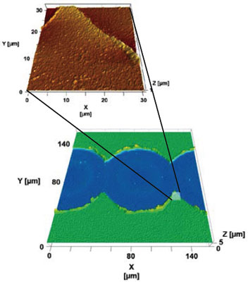
| Laser lines for interconnecting solar cell modules: a) AFM scan, image size: 30 µm x 30 µm, Z-height: 1973 nm; b) Confocal image, image size: 158 µm x 158 µm, Z-height: 8.194 µm | |
| By B. L. Holmes, A. Thöne, Bruker Nano, Herzogenrath, Germany | |
|
Become a Spotlight guest author! Join our large and growing group of guest contributors. Have you just published a scientific paper or have other exciting developments to share with the nanotechnology community? Here is how to publish on nanowerk.com. |
|