| Posted: Mar 08, 2010 | |
Photonic crystals allow the fabrication of miniaturized spectrometers |
|
| (Nanowerk Spotlight) Spectrometers are used in materials analysis by measuring the absorption of light by a surface or chemical substance. These instruments measure properties of light over a specific portion of the electromagnetic spectrum. In conventional spectrometers, a diffraction grating splits the light source into several beams with different propagation directions according to the wavelength of the light. Thus, to achieve sufficient spatial separation for intensity measurements at a small slit, a long light path – i.e., a large instrument – is required. | |
| However, for lab-on-a-chip or microTAS (total analysis system) applications, the spectrometer must be integrated into a sub-centimeter scale device to produce a stand-alone platform. To achieve this, researchers at the Korea Advanced Institute of Science and Technology (KAIST) propose a new paradigm in which the spectrometer is based on an array of photonic crystals with different bandgaps. | |
| Photonic crystals – also known as photonic band gap material – are similar to semiconductors, only that the electrons are replaced by photons (i.e. light). By creating periodic structures out of materials with contrast in their dielectric constants, it becomes possible to guide the flow of light through the photonic crystals in a way similar to how electrons are directed through doped regions of semiconductors. The photonic band gap (that forbids propagation of a certain frequency range of light) gives rise to distinct optical phenomena and enables one to control light with amazing facility and produce effects that are impossible with conventional optics. | |
| "Because photonic crystals reflect light of different wavelengths selectively depending on their bandgaps, we can generate reflected light spanning the entire wavelength range for analysis at different spatial positions using patterned photonic crystals," Seung-Man Yang, Director of the National Creative Research Initiative Center for Integrated Optofluidic Systems and Professor of the Department of Chemical & Biomolecular Engineering at KAIST, tells Nanowerk. "Therefore, when the light source impinges on the patterned photonic crystals, we can construct the spectrum using the reflection intensity profile from the constituent photonic crystals." | |
| To demonstrate this new concept based on patterned photonic crystals, Yang and his group used non-close-packed colloidal crystals of silica particles dispersed in photocurable resin. Due to the repulsive interparticle potential, monodisperse silica particles spontaneously crystallize into non-close-packed face-centered cubic (fcc) structures at volume fractions above 0.1. Therefore, the particle volume fraction determines both the lattice constant and the bandgap position. | |
 |
|
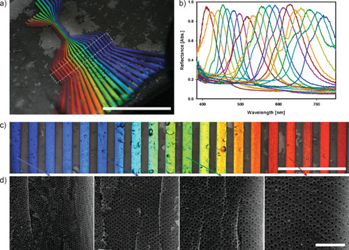
| a) Optical image of an ETPTA film containing porous photonic crystal stripe patterns with 20 different bandgaps. b) Reflectance spectra from the 20 strips. c) Optical microscope image of the middle region with the parallel stripe pattern (denoted as white-dotted box in a). d) Cross-sectional SEM images of first, sixth, eleventh and seventeenth strips. The scale bars in a, c and d are 1 cm, 2mm and 2 µm, respectively. (reprinted with permission from Wiley-VCH Verlag) | |
| Reporting their findings in a recent issue of Advanced Materials ("Integration of Colloidal Photonic Crystals toward Miniaturized Spectrometers"), the KAIST team has demonstrated the integration of colloidal photonic crystals with 20 different bandgaps into freestanding films (prepared by soft lithography), and their application as a spectrometer. | |
| Yang explains that the team was able to precisely control the photonic bandgap by varying the particle size and volume fraction. | |
| "The prepared colloidal composite structures showed high physical rigidity and chemical resistivity" he says. "The composite structure is suitable for spectroscopic use due to the small full widths at half maximum (FWHMs) of the reflectance spectra, which mean that there is little overlap of the reflectance spectra of neighboring photonic crystal strips." | |
| "On the other hand" says Yang, "porous photonic crystals showed large FWHMs and high reflectivities, which should prove useful in many practical photonic applications that require high optical performance and physical rigidity as well as simple and inexpensive preparation." | |
| In addition to fabricating miniaturized spectrometers, which can for instance be integrated into small lab-on-a-chip devices, these integrated photonic crystals can be potentially used for tunable band reflection mirrors, optical switches, and tunable lasing cavities. Moreover, patterned photonic crystals with RGB colors are well-suited for use in reflection-mode microdisplay devices. | |
| Yang points out that, although the spectrometric resolution can be reduced by employing the smaller bandgap interval and photonic bandwidth, there is a limitation. "Now, we are studying photonic crystals with continuous modulation of bandgap position. We expect that the photonic crystals can reduce the resolution to 0.01 nm." | |
 By
Michael
Berger
– Michael is author of three books by the Royal Society of Chemistry:
Nano-Society: Pushing the Boundaries of Technology,
Nanotechnology: The Future is Tiny, and
Nanoengineering: The Skills and Tools Making Technology Invisible
Copyright ©
Nanowerk LLC
By
Michael
Berger
– Michael is author of three books by the Royal Society of Chemistry:
Nano-Society: Pushing the Boundaries of Technology,
Nanotechnology: The Future is Tiny, and
Nanoengineering: The Skills and Tools Making Technology Invisible
Copyright ©
Nanowerk LLC
|
|
|
Become a Spotlight guest author! Join our large and growing group of guest contributors. Have you just published a scientific paper or have other exciting developments to share with the nanotechnology community? Here is how to publish on nanowerk.com. |
|