| Posted: Apr 21, 2010 | |
Imaging the electrostatic force with an atomic force microscope |
|
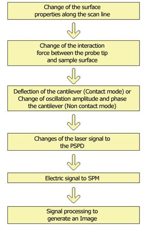
| (Nanowerk Spotlight – Application Note) Most of the material properties investigated by atomic force microscopy AFM are acquired by processing the deflection signal of the cantilever as depicted in Figure 1, which is applied to Electrostatic Force Microscopy (EFM) measurements as well. | |
| For EFM, the sample surface properties would be electrical properties and the interaction force will be the electrostatic force between the biased tip and the sample. | |
| However, in addition to the electrostatic force, the van der Waals forces between the tip and the sample surface are always present. The magnitude of these van der Waals forces change according to the tip-sample distance, and are therefore used to measure the surface topography. | |
 |
|
| Figure 1. Schematic diagram of the surface property measurement by the advanced XE modes. | |
| Hence, the obtained signal contains both information of surface topography (called ‘Topo signal’) and information of surface electrical property (called ‘EFM signal’) generated by the van der Waals and electrostatic forces, respectively. The key to successful EFM imaging lies in the separation of the EFM signal from the entire signal. EFM modes can be classified according to the method used to separate the EFM signal. | |
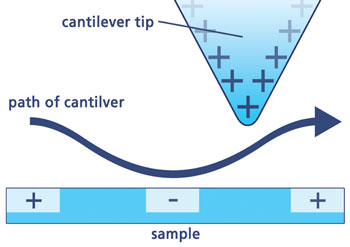
| Electrostatic Force Microscopy (EFM) of Park System's XE-series maps electric properties on a sample surface by measuring the electrostatic force between the surface and a biased AFM cantilever. EFM applies a voltage between the tip and the sample while the cantilever hovers above the surface, not touching it. The cantilever deflects when it scans over static charges, as depicted in Figure 2. | |
 |
|
| Figure 2. EFM maps locally charged domains on the sample surface. | |
| EFM images contain information about electric properties such as the surface potential and charge distribution of a sample surface. EFM maps locally charged domains on the sample surface, similar to how MFM plots the magnetic domains of the sample surface. The magnitude of the deflection, proportional to the charge density, can be measured with the standard beam-bounce system. Thus, EFM can be used to study the spatial variation of surface charge carrier. For instance, EFM can map the electrostatic fields of an electronic circuit as the device is turned on and off. This technique is known as “voltage probing” and is a valuable tool for testing live microprocessor chips at the sub-micron scale. | |
| Four different EFM modes, distinguished by the method which the surface electrical information is obtained, are provided by XE-series AFM. These are Standard EFM, Park Systems’s own patented Dynamic-Contact EFM (DC-EFM), Piezoelectric Force Microscopy (PFM), and Scanning Kelvin Probe Microscope (SKPM). | |
| Standard EFM | |
| The standard EFM of the XE-series is based on the two facts. One fact is that van der Waals forces and electrostatic forces have different dominant regimes. van der Waals forces are proportional to 1/r6, while electrostatic forces are proportional to 1/r2. Thus, when the tip is close to the sample, van der Waals forces are dominant. Whereas the van der Waals forces rapidly decrease and the electrostatic forces become dominant, as the tip is moved away from the sample. | |
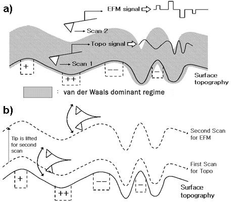
| The other fact is that the topography line is acquired by keeping the tip-sample distance constant, which equals the line of constant van der Waals force. In the Force Range technique, the first scan is performed by scanning the tip in the region where the van der Waals force is dominant for topography image. Then, the tip-sample distance is varied to place the tip in the region where the electrostatic force is dominant and scanned for EFM image as shown in Figure 3(a). | |
 |
|
| Figure 3. The schematics of (a) Force Range technique and (b) two pass technique. | |
| In the Two Pass technique, the first scan is performed to obtain the topography by scanning the tip near the surface as it is done in NC-AFM, in the region where the van der Waals forces are dominant. In the second scan, system lifts the tip and increases the tip-sample distance in order to place the tip in the region where electrostatic forces are dominant. The tip is then biased and scanned without feedback, parallel to the topography line obtained from the first scan as shown in Figure 3 (b), therefore maintaining constant tip-sample distance. | |
| Since the topography line is the line of constant van der Waals force, the van der Waals forces applied to the tip during the second scan are constant. Thus, the only source of the signal change will be the change of the electrostatic force. So, from the second scan, a topography free EFM signal can be obtained. | |
 |
|
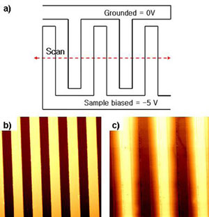
| Figure 4. Standard sample is made of two micro comb shaped electrodes with one’s teeth lying between the other’s (a). Topography image (b) shows that neighboring teeth are of same height but EFM Phase image (c) shows that neighboring teeth of same height differ in surface potential. | |
| By Park Systems. | |
|
Become a Spotlight guest author! Join our large and growing group of guest contributors. Have you just published a scientific paper or have other exciting developments to share with the nanotechnology community? Here is how to publish on nanowerk.com. |
|